Altera ALTDQ_DQS2 User Manual
Page 55
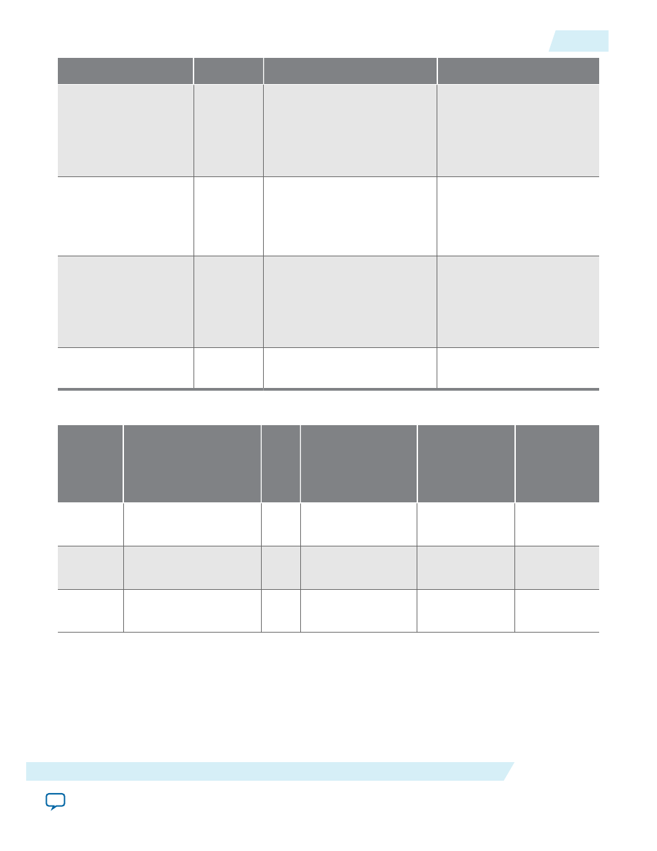
Legend in
Bit
External Bit Name
Description
D
17..15
readfifomode
Connects to the dynfifomode
port of input register read
FIFO block. The read FIFO
can be configured as a read
FIFO or a Unified SerDes
Block.
E
19..18
readfiforeadclockselect
Connects to the clksel port of
the read FIFO clock select
block. This controls the read
FIFO Read clock source
Select.
F
20
outputhalfratebypass
Sets the multiplexer in the
output enable and output
data path logic to
dynamically bypass the half-
rate to full-rate DDIO. Used
only with the hard PHY.
—
24..21
Not mapped to any port
Unconfigurable bits. Always
set bits to its default value.
Table 17: I/O Configuration Block Bit Sequence for Arria V and Cyclone V Devices
Bit
Bit Name
Defaul
t
Value
(Binar
y)
Min. Value
Max. Value
Inc. Value
4..0
padtoinputregisterdelayset‐
ting
0
intrinsic delay
775 ps + intrinsic
delay
25 ps
9..5
outputenabledelaysetting
0
intrinsic delay
775 ps + intrinsic
delay
25 ps
14..10
outputregdelaysetting
0
intrinsic delay
775 ps + intrinsic
delay
25 ps
UG-01089
2014.12.17
I/O Configuration Block Bit Sequence for Arria V and Cyclone V Devices
55
ALTDQ_DQS2 IP Core User Guide
Altera Corporation