Altera ALTDQ_DQS2 User Manual
Page 48
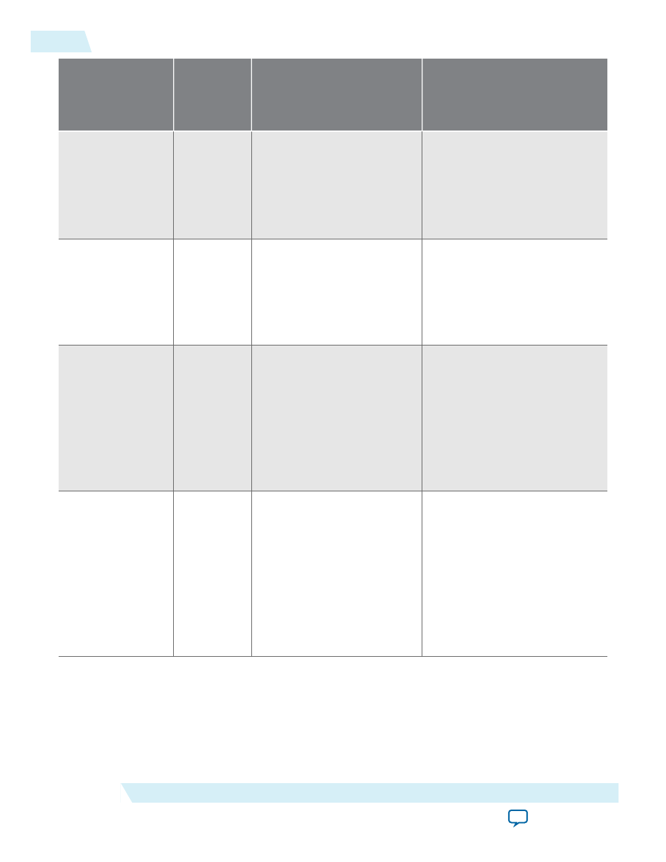
Legend in
Bit
Bit Name
Description
T
88..87
dqsinputphasesetting
Connects to the phasectrlin port
of the DQS delay chain block.
To control the phase selection for
the DQS delay chain.
The frequency range that this
works at is 300 MHz to 800 MHz.
U
89
enadqsphasetransferreg
Connects to the enaphasetrans‐
ferreg port of the output
alignment block (in the DQS
output path and OE path) to
allow an additional negative
edge-triggered register to be
used.
V
90
enaoutputphasetransferreg
Connects to the enaphasetrans‐
ferreg port of the output
alignment block (in the DQ
output path and OE path) to
allow an additional negative
edge-triggered register to be
added to the output data or
output enable path to satisfy the
setup or hold time requirement
for the phase transfer.
W
93..91
enadqscycledelaysetting
Connects to the enaoutputcycle‐
delay port of the output
alignment block (in the DQS
output path and OE path) to
allow additional registers to be
enabled in the output alignment
block of the output data or
output enable path of a DQS I/O.
This is normally used to adjust
the phase of the write-leveled
OCT or output data signal.
48
DQS Configuration Block Bit Sequence for Arria V GZ and Stratix V Devices
UG-01089
2014.12.17
Altera Corporation
ALTDQ_DQS2 IP Core User Guide