Blocks in dq and dqs data input path – Altera ALTDQ_DQS2 User Manual
Page 19
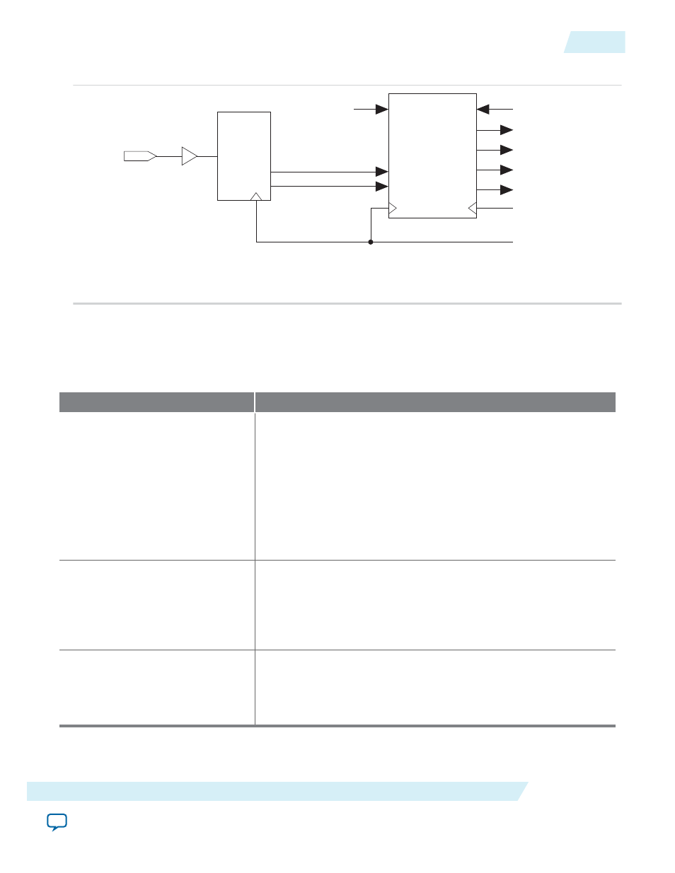
Figure 9: Data Input Path for Arria V, Cyclone V, and Stratix V Devices
DATAIN
Delay
Chain
DDIO
In
FIFO REN Logic
DATAOUT[0]
DATAOUT[1]
DATAOUT[2]
DATAOUT[3]
HR or FR Clock
DQS from DQS Logic
FIFO WREN
Logic
Read
FIFO
WREN
REN
This figure is applicable to Stratix V devices because Stratix V devices support optional hard read FIFO.
Blocks in DQ and DQS Data Input Path
The following table lists the blocks in the DQ and DQS input paths.
Table 4: Blocks in DQ and DQS Input Path
Block Name
Description
DQS enable
• Represents the AND-gate control on the DQS input that grounds
the DQS input strobe when the strobe goes to Hi-Z after a DDR
read postamble. The DQS enable block enables the registers to
allow enough time for the DQS delay settings to travel from the
DQS phase-shift circuitry or core logic to all the DQS logic blocks
before the next change.
• For more information about the DQS enable block, refer to the
“Update Enable Circuitry” in the External Memory Interfaces
chapter in the respective device handbook.
DQS enable control
• Represents the circuitry that controls the DQS enable block. A
DQS enable control block controls each DQS enable block.
• For more information about the DQS enable control block, refer
to the “DQS Postamble Circuitry” in the External Memory
Interfaces chapter in the respective device handbook.
DQS delay chain
• Represents the delay chains that delay signals.
• For more information about the DQS delay chain block, refer to
“DQS Delay Chain” in the External Memory Interfaces chapter in
the respective device handbook.
UG-01089
2014.12.17
Blocks in DQ and DQS Data Input Path
19
ALTDQ_DQS2 IP Core User Guide
Altera Corporation