Stratix v design example – Altera ALTDQ_DQS2 User Manual
Page 59
Bit
External Bit Name
Defaul
t Value
(Binary
)
Min. Value
Max. Value
Inc. Value
21..17
dqsbusoutdelaysetting
0
intrinsic delay
775 ps +
intrinsic delay
25 ps
22
postamblephaseinvert
0
0 = Non-invert
1 = Invert
24..23
postamblephasesetting
0
00 = 0°
01 = 45°
10 = 90°
11 = 135°
29..25
Not mapped to any port
0
—
Related Information
•
•
Example Usage of Dynamic Reconfiguration for ALTDQ_DQS2
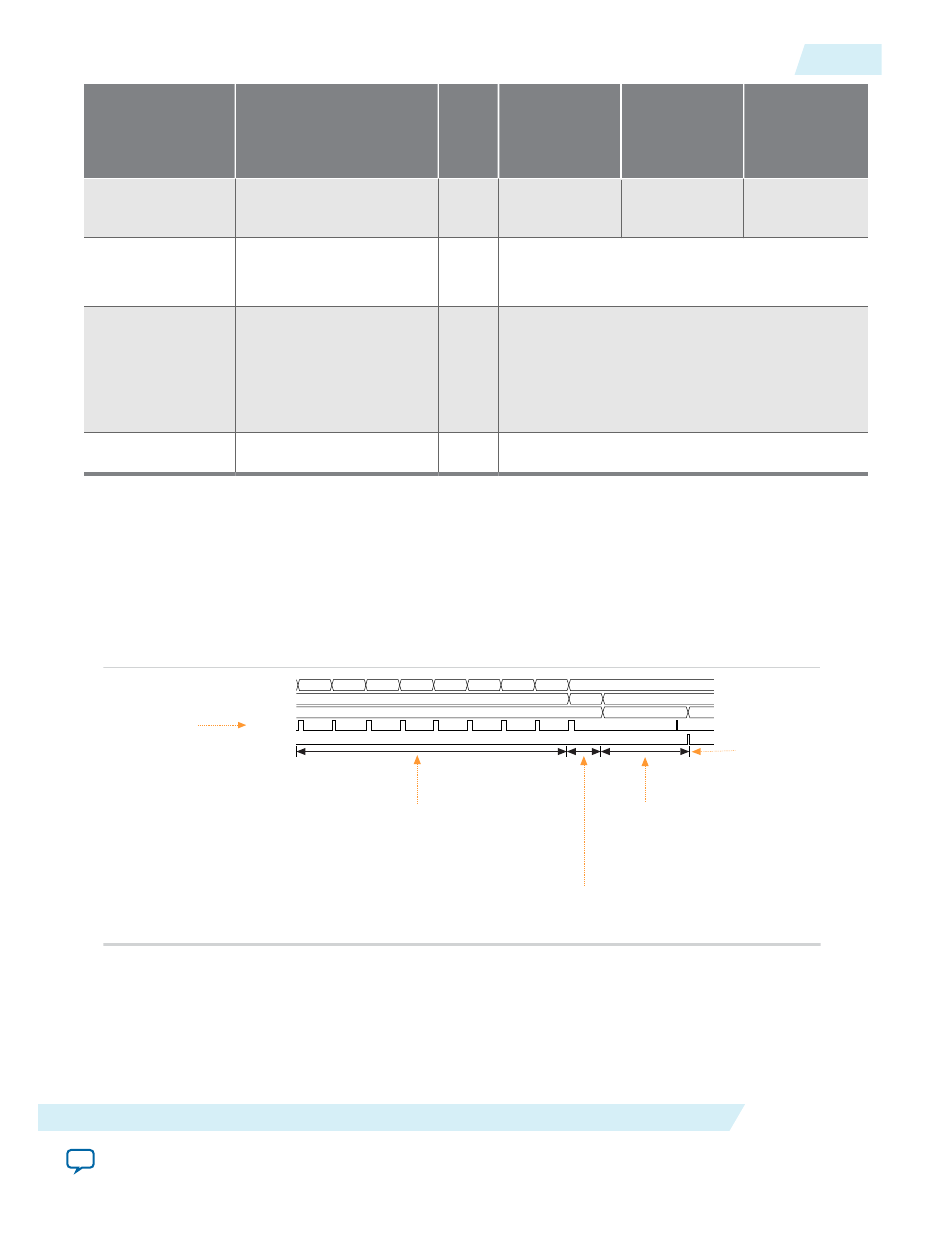
Figure 20: Example Usage of Dynamic Reconfiguration
When the scanning process begins, assert each config_io_ena
bit for 40 cycles to enable the 40 bits config_data (based on the
I/O configuration block bits) for each DQ I/O. Each DQS group
consists of a configuration block per one DQ pin. The
config_ena_io is eight bit because the DQ pin width is set to 8.
Assert config_dqs_io_ena for 40 cycles to
shift the 40 bits config_data (based on I/O
configuration block bits) for the DQS pin.
Assert config_dqs_ena for 101 cycles to shift
the 101 bits config_data (based on DQS
configuration block bits) for the DQS logic.
Assert config_update for
one cycle. The scan chain
process is complete.
config_ena_io[7:0]
config_dqs_io_ena[0:0]
config_dqs_ena[0:0]
config_data
config_update
01
02
04
08
10
20
80
00
1
0
0
1
0
0
40
The bitstream for the config_data
signal is LSB first (from LSB to
MSB).
Stratix V Design Example
This section describes how to instantiate the ALTDQ_DQS2, ALTERA_PLL, ALTDLL, ALT_OCT IP
cores using the Top_SV_13.0sp1.qar design example.
UG-01089
2014.12.17
Example Usage of Dynamic Reconfiguration for ALTDQ_DQS2
59
ALTDQ_DQS2 IP Core User Guide
Altera Corporation