Dqs enable control, Simulation results – Altera ALTDQ_DQS2 User Manual
Page 91
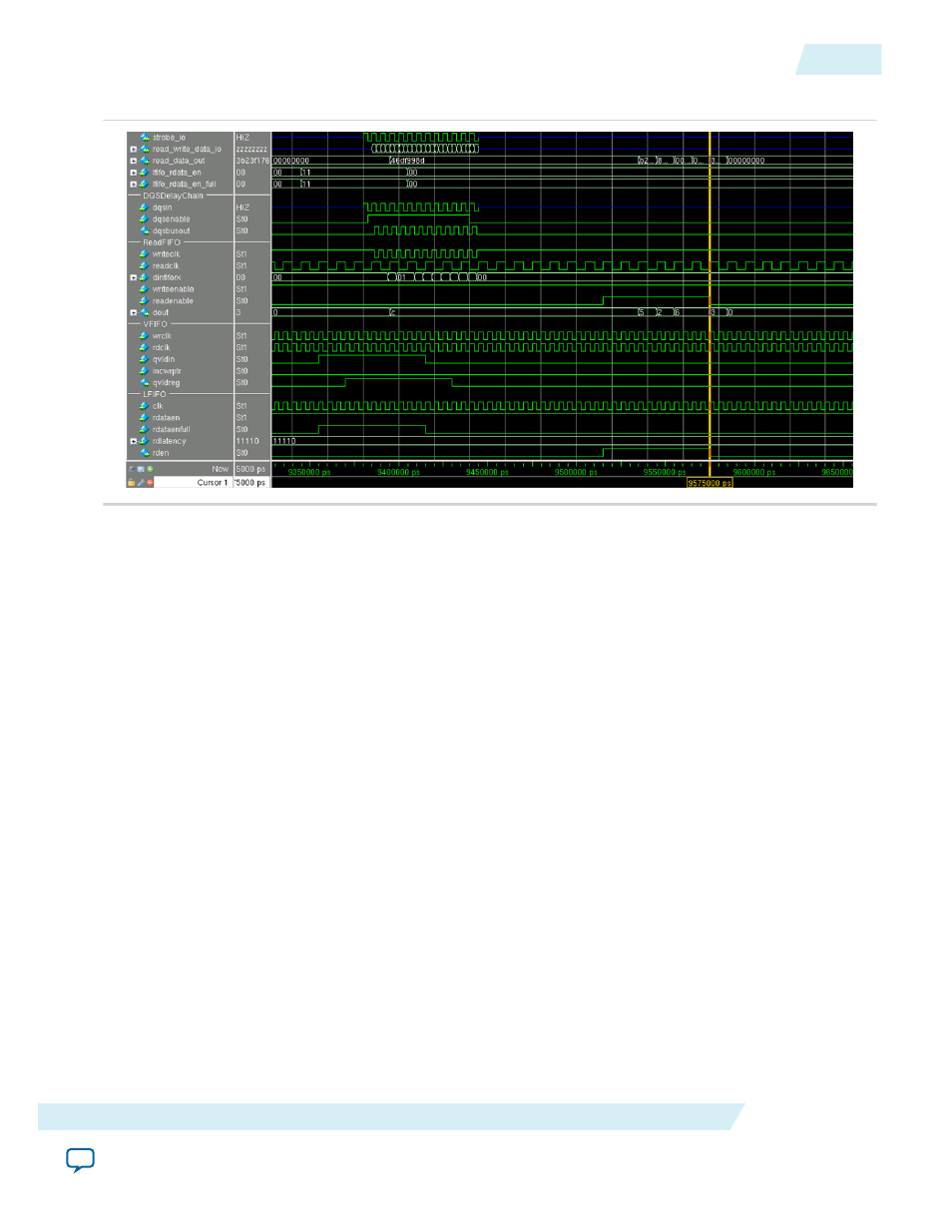
Figure 64:
Note: The write enable (
we
) and read enable (
re
) signals of the hard read FIFO are different from the
wrreq
and
rdreq
signals of the DCFIFO. In DCFIFO, the data are only available at the FIFO
output ports when the
rdreq
signal is asserted. In hard read FIFO, the
we
signal controls when to
advance the write address counter while the
re
signal controls when to advance the read address
counter. When the read and write address pointers are the same, write data appear at the read port
as soon as a write operation is completed. This explains why we see the first written data available
almost immediately at the FIFO output port. When the signal is asserted, it will advance to the next
read address, and then only the second written data is available at the FIFO output port.
Note: Beginning from the Quartus II software version 13.1, the
lfifo_rdata_en
and
lfifo_rdata_valid
signals will be removed.
DQS Enable Control
The goal of DQS enable calibration is to find settings that satisfy the following conditions:
• The DQS enable signal rises before the first rising edge of DQS.
• The DQS enable signal is high after the second-last falling edge of DQS.
• The DQS enable signal falls before the last falling edge of DQS.
The ideal position for the falling edge of the DQS enable signal is centered between the second-last and
last falling edges of DQS.
Related Information
•
Simulation Results
The following figure shows the simulation results in the message panel. lf the simulation failed, it is due to
the data sent/received at the ALTDQ_DQS2 is not the same as the expected ones.
UG-01089
2014.12.17
DQS Enable Control
91
ALTDQ_DQS2 IP Core User Guide
Altera Corporation