Hard read fifo – Altera ALTDQ_DQS2 User Manual
Page 71
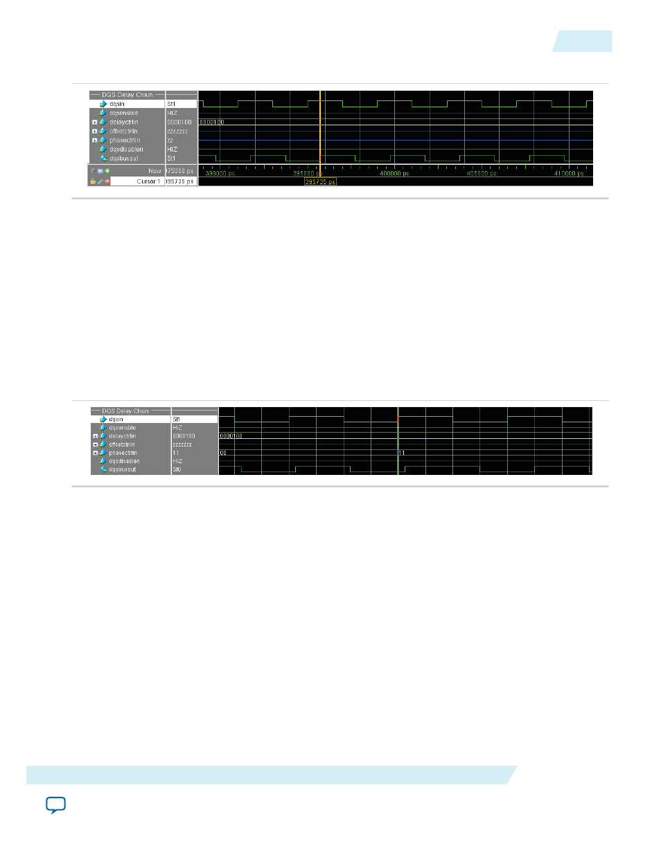
Figure 38: DQS Delay Chain Waveform
However, when you enable the dynamic configuration feature,
phasectrlin
(which is set via the
dqsinputphasesetting
port of the DQS configuration) determines the phase applied to the
dqsbusout
output.
Observe the following waveform. Before dynamic configuration,
phasectrlin
was set to 2'b00 and the
shift between
dqsin
and
dqsbusout
is about 245 ps (should be 0 ps). Meanwhile after performing
dynamic configuration,
phasectrlin
was set to 2'b11 and the shift between
dqsin
and
dqsbusout
is
about 980 ps (should be 735 ps, which is 67.5°). This is consistent with the settings in
.
Note: There is a simulation error for the
phasectrlin
. The current incorrect modeled setting is as
follows: 00 = 45°, 01 = 90°, 10 = 135°, 11 = 180°. It is scheduled to be fixed at QII 14.0, to be
modeled correctly as: 00 = 0°, 01 = 45°, 10 = 90°, 11 = 135°
Figure 39: DQS Delay Chain Waveform
Hard Read FIFO
As seen in the waveform below, the incoming read data is available on
read_write_data_io
between
19.171 µs and 19.219 µs. The capture DDlO block captures input data (DQ) on the rising and falling edges
of the capture clock (DQS). For Stratix V devices, the capture DDlO block feeds the hard read FlFO or
bypasses the hard read FlFO and goes directly to the core. The data transfer from the capture DDlO block
and the next stage is referred to as zero-cycle transfer. This means that the transfer must happen on the
same clock edge.
Note: To ensure correct timing analysis, use the
set_multicycle
SDC command.
This design example uses a hard read FIFO. When the first data is available at 19.174 µs, the
v/i/o_qvld
is asserted. This signal passes through the
write_enable_ctrl
of the DDlO OUT before driving the read
enable port of the read FIFO. As the write enable signal of the read FlFO block is asserted, data is written
to the read FlFO between 19.174 µs and 19.222 µs . The
l/i/o_rden
, which is connected to the read
enable port of the read FlFO block through a fifo_enable block, is then asserted between 19.219 µs and
19.267 µs. Read data is available in the core between 19.179 µs and 19.275 µs on
read_data_out
. You may
further optimize the timing to read the read FlFO by adjusting the
l/i/o_rden
to create enough space
between the read and write pointers in the read FlFO to maximize the throughput.
UG-01089
2014.12.17
Hard Read FIFO
71
ALTDQ_DQS2 IP Core User Guide
Altera Corporation