Simulation results, Sdc walkthrough – Altera ALTDQ_DQS2 User Manual
Page 73
the write address counter, while the
re
signal controls when to advance the
readaddress
counter.
When the read/write address pointers are the same, write data appears at the read port as soon as
the write operation is completed. When the
re
signal is asserted, it will advance to the next read
address and then only the second written data is available at the FIFO output port.
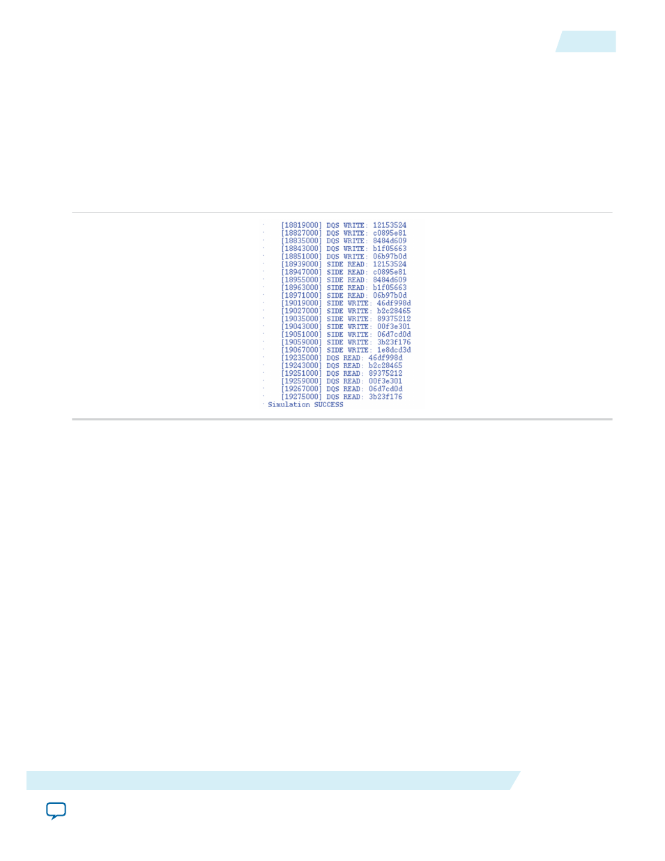
Simulation Results
The following figure shows the simulation results in the message panel. lf the simulation failed, it is due to
the data sent/received at the ALTDQ_DQS2 is not the same as the expected ones.
Figure 42: Simulation Results
SDC Walkthrough
To create a new .sdc, follow these steps:
1. Constrain the clocks coming into the FPGA with a
create_clock
command. The following command
creates the base clock for the input clock port driving the PLL:
create_clock -name refclk -period 10.000 [get_ports {refclk}]
2. Create the generated clocks for the PLL with the following command:
derive_pll_clocks
3. Constraint the virtual input clock (for incoming DQS strobe) and the
capture_strobe_in
port. ln this
example design, it is based on a 250 MHz input clock, with a 50% duty cycle, where the first rising edge
occurs at 0 ns.
create_clock -name virtual_dqs_in -period 4.000
create_clock -name dqs_in -period 4.000[get_ports {capture_strobe_in}]
4. lncoming data is edge aligned to the DQS strobe, and minimum and maximum input delay is assumed
to be ± 0.3ns in this design example. You must modify constraints to reflect the data and clock
relationship in the system. Use the
-add
option to add the user-defined delay constraint instead of
overriding previous constraints.
set_input_delay -clock {virtual_dqs_in} -max -add_delay 0.300 [get_ports
{read_write_data_io[*]}]
UG-01089
2014.12.17
Simulation Results
73
ALTDQ_DQS2 IP Core User Guide
Altera Corporation