Altdq_dqs2 ports – Altera ALTDQ_DQS2 User Manual
Page 24
Block Name
Description
DDR output registers
Represents the DDIO registers that transfer DDR signals
from the core to the DQ/DQS pins.
Related Information
•
•
•
DQ and DQS Output Path for Arria V and Cyclone V Devices
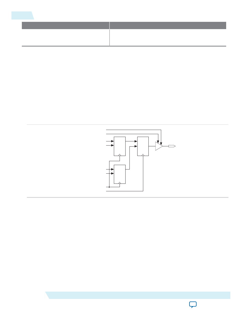
The data output path for Arria V and Cyclone V families is similar to the output paths for Stratix V and
earlier families, except for the output phase alignment registers. These registers are not available in Arria
V and Cyclone V devices and do not support leveled interfaces.
The following figure shows the DQ and DQS output path for Arria V and Cyclone V devices.
Figure 14: DQ and DQS Output Path for Arria V and Cyclone V Devices
DATAOUT
DDIO
Out
DATAOUT[0]
DATAOUT[1]
DATAOUT[2]
DATAOUT[3]
DDIO
Out
DDIO
Out
CLK_HR
CLK_FR
OCT from DQS Logic
OE from Output Enable Path
You must connect the ALTDQ_DQS2 IP core to the ALTOCT, ALTDLL, and ALTERA_PLL IP cores to
utilize their features.
Related Information
•
Instantiating IP cores
ALTDQ_DQS2 Ports
The following figure shows the data strobe, data, termination control, PLL, DLL, hard FIFO, and dynamic
configuration ports of the IP core.
24
DQ and DQS Output Path for Arria V and Cyclone V Devices
UG-01089
2014.12.17
Altera Corporation
ALTDQ_DQS2 IP Core User Guide