Dqs read operation, Dqs delay chain, For the results of this settings, refer to – Altera ALTDQ_DQS2 User Manual
Page 70
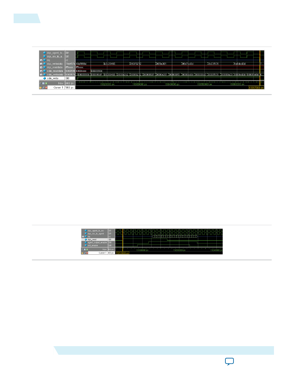
The following figure shows the waveform for the side write operation.
Figure 36: Side Write Operation Waveform
Note: The incoming data at
dq
is edge-aligned to the
dqs_agent_to_ios
.
DQS Read Operation
Between 19.227 µs and 19.275 µs when the
dqs_readdata_valid
signal is held high, data validation is
done by comparing data received by the ALTDQ_DQS2 core (
read_data_out
) against the content in the
check/i/o
.
ln Stratix V devices, you can choose to enable or disable the hard read FlFO. The read FlFO is in every
input data paths. The read FlFO handles full-rate and half-rate conversion only. This example design uses
the hard read FlFO. The testbench determines the timing to assert the write enable and read enable ports
via the
v/i/o_qvld
and
l/i/o_rden
. ln an actual application, you must design your own logic to do so.
The DQS driver begins the DQS read operation when the
dqs_read
signal is asserted at 19.139 µs, for the
entire length of the desired read burst, which in this case is 12 full-rate cycles. The DQS agent also receive
the read command, and is ready to send out data. After a specific latency, the
agent_output_enable
signal is asserted beginning from 19.167 µs to 19.219 µs. During this period, the DQS agent drives clock
and data lines of the external memory interface. The
oct_enable
signal is asserted between 19.155 µs and
19.211 µs. The incoming data (
dq
) is edge-aligned to the clock (
dqs_agent_to_ios
).
Figure 37: DQS Read Operation Waveform
DQS Delay Chain
Because the DQS enable block is not applicable for this example design, the
dqsenable
signal is held at
Hi-Z at all time. The
dqsbusout
signal is the delayed
dqsin
signal that drives to the dedicated DQS clock
network to clock the DQ capture registers, so that data are captured at the center of the eye. If you disable
the dynamic configuration feature, you should see a 67.5° phase shift (or 735 ps) between
dqsin
and
dqsbusout
, as expected due to the settings in
. The following figure shows that the
phasectrlin
signal is held at Hi-Z.
70
DQS Read Operation
UG-01089
2014.12.17
Altera Corporation
ALTDQ_DQS2 IP Core User Guide