Blocks in dq and dqs output path – Altera ALTDQ_DQS2 User Manual
Page 23
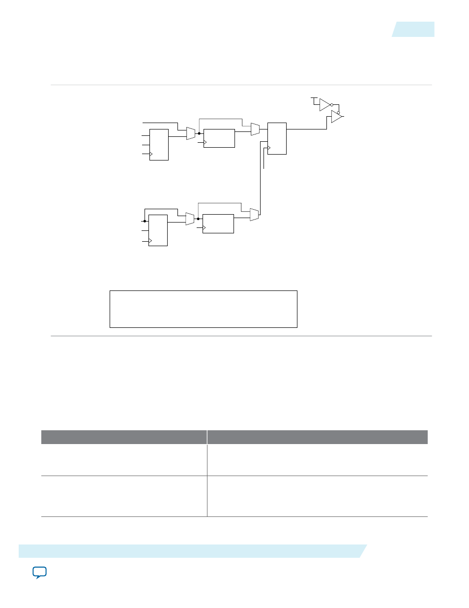
The following figure shows the DQ and DQS output path for additional DQ pins usage, where y = 0 to
(m-1) and m= the number of DQ pins
Figure 13: DQ and DQS Output Path (for Additional DQ Pins Usage) for Stratix V Devices
extra_write_data_in[3m+y]
hr_clock_in
datain dataout
HI OUT
extra_write_data_in[2m+y]
HI OUT
hr_clock_in
extra_write_data_in[m+y]
datain dataout
HI OUT
extra_write_data_in[y]
LO
Half-rate to
single-rate output
enable registers
Output phase
alignment registers
Alignment
clock
0
1
Alignment
clock
Half-rate to
single-rate
output registers
Output phase
alignment registers
0
1
0
1
0
1
VCC
DDR output registers
extra_write_data_out[y]
Write clock
LO
LO
extra_write_data_in[y]
(to DQ pin)
Alignment
clock
Write clock
The alignment clock comes from the write-leveling delay chains.
The write clock comes from the PLL or the write-leveling delay chains.
Related Information
•
Blocks in DQ and DQS Output Path
The following table lists the blocks in the DQ and DQS output path.
Table 5: Blocks in the DQ and DQS Output Path
Block Name
Description
Half-rate to single-rate output enable
registers
Represents a group of registers that convert half-rate data to
single-rate data.
Output phase alignment registers
Represents the circuitry required to phase shift the DQ-
output signals. Use this block for write-leveling purposes in
DDR3 SDRAM interfaces.
UG-01089
2014.12.17
Blocks in DQ and DQS Output Path
23
ALTDQ_DQS2 IP Core User Guide
Altera Corporation