Dq and dqs output path, Dq and dqs output path for stratix v devices – Altera ALTDQ_DQS2 User Manual
Page 22
The determination of the correct latencies to implement at each of these FIFOs is important and cannot
be done during compilation. When you attempt to implement your own custom memory solution, you
must also implement some form of calibration algorithm.
To determine if the data coming from the read FIFO is valid, you must implement the read data valid
latency in soft logic.
Related Information
DQ and DQS Output Path
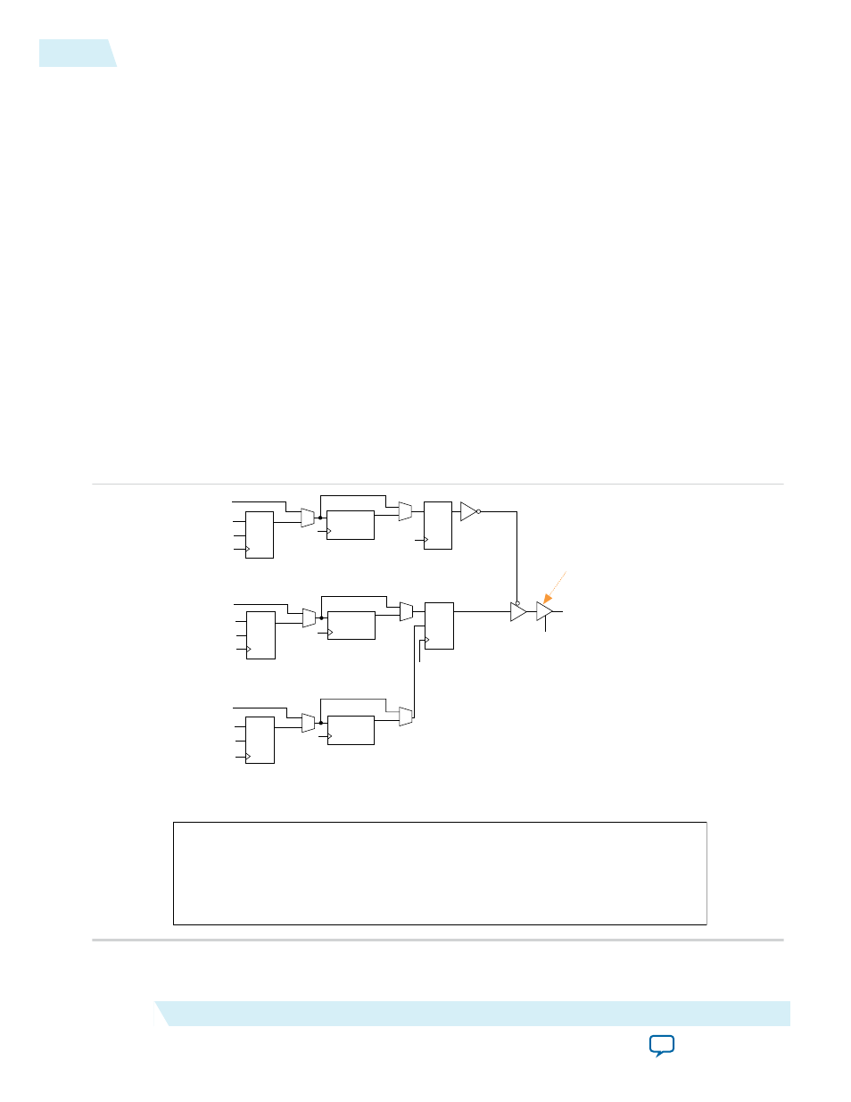
The DQ and DQS output path sends the DQ and DQS signal to the external device during write
operations.
DQ and DQS Output Path for Stratix V Devices
The following figure shows the output path where n = the number of DQ pins and x = 0 to (n-1). is only
applicable for Stratix V devices.
Note: This figure is only applicable for Stratix V devices. For Arria V and Cyclone V DQ and DQS output
.
Figure 12: DQ and DQS Output Path for Stratix V Devices
write_oe_in[2x]
hr_clock_in
datain dataout
LO OUT
write_oe_in[2x+1]
D
Q
write_data_in[3n+x]
hr_clock_in
HI OUT
write_data_in[n+x]
HI OUT
hr_clock_in
write_data_in[2n+x]
datain dataout
HI
Q
write_data_in[x]
LO
HI
Half-rate to
single-rate output
enable registers
Output phase
alignment registers
Alignment
clock
Write
clock
0
1
LO
0
1
datain dataout
0
1
DDR output registers
Write
clock
Alignment
clock
write_data_out[x]
Half-rate to
single-rate
output registers
Alignment
clock
Half-rate to
single-rate
output registers
Output phase
alignment registers
Output phase
alignment registers
0
1
0
1
0
1
Series termination
control
LO
write_oe_in[x]
(to DQ pin)
write_data_in[x]
write_data_in[n+x]
DFF
Alignment
clock
Write
clock
Series termination
control
The alignment clock comes from the write-leveling delay chains. For more information, refer to “Leveling Circuitry”
section in the External Memory Interfaces in Stratix V Devices chapter in the Stratix V Device Handbook.
The write clock comes from the PLL or the write-leveling delay chains. For more information, refer to “Leveling
Circuitry” section in the External Memory Interfaces in Stratix V Devices chapter in the Stratix V Device Handbook.
The series termination control connects to the ALTOCT megafunction.
For bidirectional DQ, the output of the buffer
connects to the read_write_data_io[x] port.
22
DQ and DQS Output Path
UG-01089
2014.12.17
Altera Corporation
ALTDQ_DQS2 IP Core User Guide