Altera ALTDQ_DQS2 User Manual
Page 53
I/O Configuration Block Bit Sequence for Arria V and Cyclone V Devices
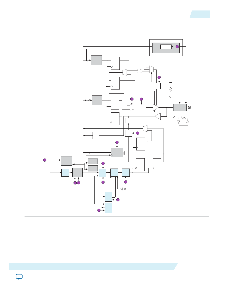
Figure 19: I/O and DQS Delay Chains for Arria V and Cyclone V Devices
4
Open Drain
Programmable
Pull-Up Resistor
4
PRN
D
Q
PRN
D
Q
PRN
D
Q
PRN
D
Q
PRN
D
Q
clkout
D5 Delay
PRN
D
Q
PRN
D
Q
D5_OCT
2
From
Core
OE from
Core
Write Data
from Core
To Core
To Core
Read Data
to Core
Read
FIFO
D3_1
Delay
Half Data
Rate Block
Half Data
Rate Block
DQS Logic Block
Dynamic OCT Control (2)
V
CCIO
D5 Delay
Output Buffer
Input Buffer
Programmable
Current Strength
and Slew Rate Control
From OCT
Calibration
Block
On-Chip
Termination
Bus Hold Circuit
D3_0
Delay
D1
Delay
Output Register
Output Register
OE Register
OE Register
Input Register
Input Register
Input Register
DQ
DQS
Delay
Chain
D4
Delay
Chain
Leveling
Delay
Chain
I
K
G
H
N M
L
D
Mode
rdclk
A
C
F
B
J
E
Read FIFO
Clock Select
DQS
T11
Gating
Delay
Chain
T11
Ungating
Delay
Chain
DQS
Enable
Control
Latency
Shifter FIFO
Data Valid
FIFO
Clock
Phase
Select
Clock Signal
from Core
Clock Select
The following table lists the I/O configuration block bit sequence, description, and settings for Arria V
and Cyclone V devices.
UG-01089
2014.12.17
I/O Configuration Block Bit Sequence for Arria V and Cyclone V Devices
53
ALTDQ_DQS2 IP Core User Guide
Altera Corporation