Maxim Integrated Ultra-High-Speed Flash Microcontroller User Manual
Page 86
6-19
Page Mode 1 Data Memory Timing–Pages 1:0 = 01b (Two Cycles) (continued)
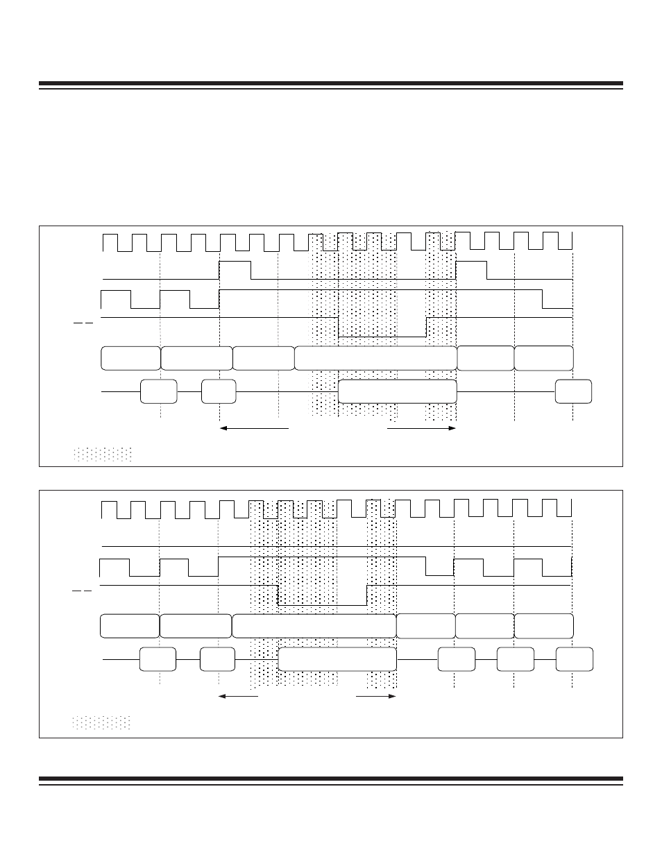
Figure 6-17 shows execution of a MOVX instruction with default stretch value = 1 (MD2:0 = 001b) from external program memory. The
most probable case, where a page-miss is needed for the MOVX instruction, is given here. However, if the MOVX address happened
to coincide with the current code execution page, a page hit would occur.
Figure 6-18 illustrates the MOVX timing that would occur if the address MSB for the MOVX data were to coincide with the code exe-
cution pages before and after the data access. Since a different MSB would not need to be latched, neither of the page-miss cycles
seen in the third diagram would occur.
Ultra-High-Speed Flash
Microcontroller User’s Guide
SYSCLK
ALE
PSEN
PORT2
LSB
LSB
MSB
LSB
MOVX MSB
MOVX LSB
MOVX DATA
PORT0
WR/RD
MOVX
INST
(PAGE HIT)
INST
(PAGE MISS)
MOVX DATA ACCESS
(PAGE MISS + 1 STRETCH CYCLE)
= STRETCH CYCLE
SYSCLK
ALE
PSEN
PORT2
PORT0
WR/RD
MOVX #1
INST
(PAGE HIT)
INST
(PAGE HIT)
INST
(PAGE HIT)
INST
(PAGE HIT)
= STRETCH CYCLE
MOVX LSB
LSB
LSB
LSB
LSB
LSB
MOVX DATA
MOVX DATA ACCESS
(PAGE HIT + 1 STRETCH CYCLE)
Figure 6-18. Two-Cycle Page Mode 1: MOVX (Three Cycles) External Code Execution - No Page Misses
Figure 6-17. Two-Cycle Page Mode 1: MOVX (Three Cycles) External Code Execution with Page Misses
Maxim Integrated