Maxim Integrated Ultra-High-Speed Flash Microcontroller User Manual
Page 74
6-7
Internal Memory Cycles
C2
C3 C4 C1 C2 C3 C4
XTAL1
ALE
Port 0
Port 2
PSEN
C1
Ext Memory Cycle
Ext Memory Cycle
MSB Add MSB Add
LSB Add Data LSB Add Data
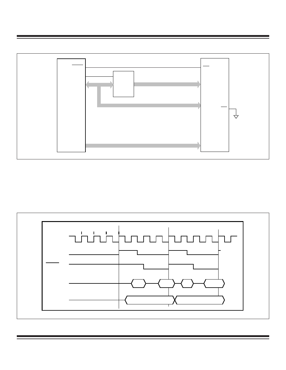
Figure 6-3. External Program Memory Access (Nonpage Mode and CD1:0 = 10b)
Figure 6-3 shows the timing relationship for internal and external nonpage mode code fetches when CD1:0 = 10b. Note that an exter-
nal program fetch takes four system clocks, and an internal program fetch requires only one system clock.
As illustrated in that same figure, ALE is deasserted when executing an internal memory fetch. The microcontroller provides a pro-
grammable user option (ALEON bit = PMR.2) to turn on the ALE signal during internal program memory operation. The ALE signal is
automatically enabled for external code fetches, independent of the setting of this bit. PSEN is asserted only for external code fetch-
es, and is inactive during internal execution.
PSEN
ALE
CK
74F373
LATCH
LSB ADDRESS
DATA BUS
MSB ADDRESS
PORT 2
(8)
(7)
64kB X 8
MEMORY
(8)
OE
CE
PORT 0
DS89C4x0
Figure 6-2. Program Memory Interconnect (Nonpage Mode)
Ultra-High-Speed Flash
Microcontroller User’s Guide
Maxim Integrated