Maxim Integrated Ultra-High-Speed Flash Microcontroller User Manual
Page 77
6-10
Ultra-High-Speed Flash
Microcontroller User’s Guide
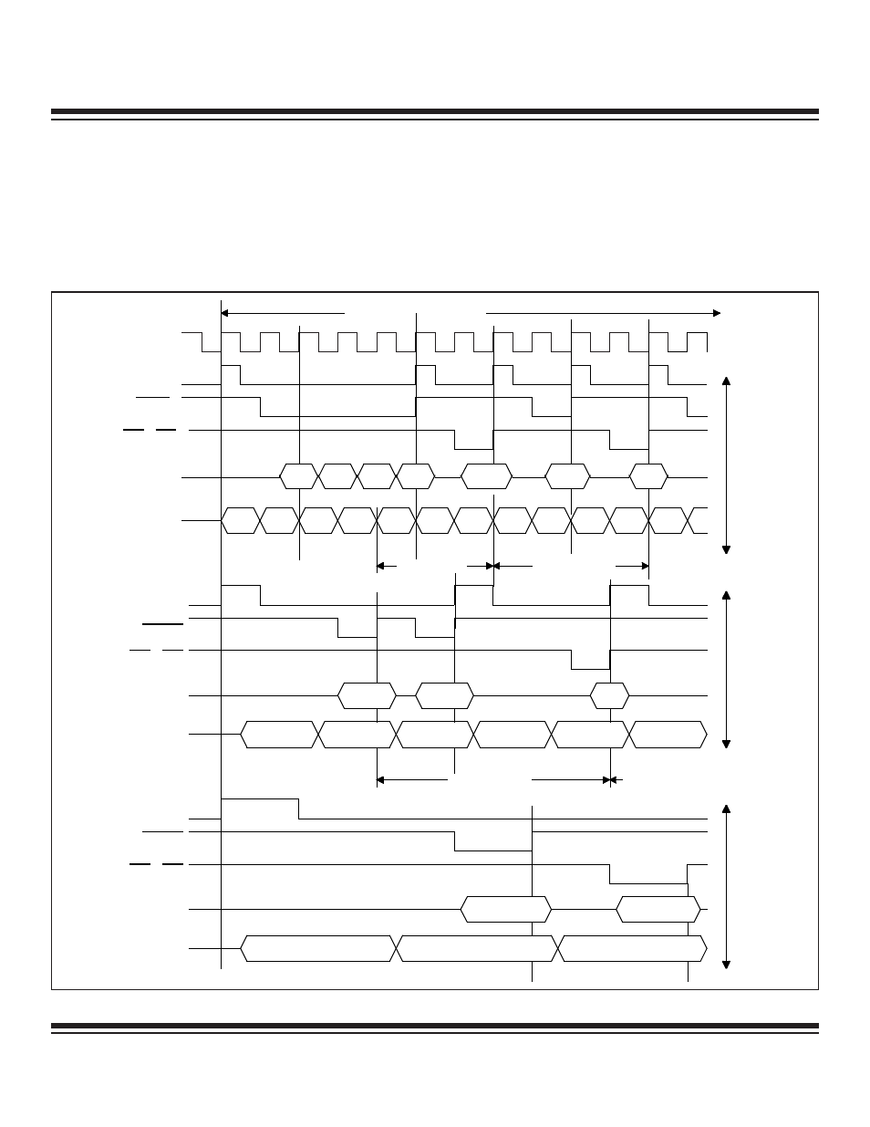
Figure 6-5 shows external memory cycles for the page mode 1 bus structure. The first case illustrates a back-to-back MOVX execu-
tion sequence for one-cycle page mode (PAGES 1:0 = 00b). PSEN remains active during page-hit cycles, and page misses are forced
during and after MOVX executions, independent of the most significant byte of the subsequent addresses. The second case illustrates
a MOVX execution sequence for two-cycle page mode (PAGES 1:0 = 01b). PSEN is active for a full clock cycle in code fetches. Note
that the page misses in this sequence are caused by changing of the most significant byte of the data address. The third case illus-
trates a MOVX execution sequence for four-cycle page mode (PAGES 1:0 = 10b). There is no page-miss in this execution cycle, as the
most significant byte of the data address is assumed to match the last program address.
Internal Memory Cycles
XTAL1
ALE
Port 0
Port 2
Data
Data
Inst
MSB
MSB
MSB
MSB
MSB LSB
LSB
LSB
LSB
LSB
LSB
Inst
Inst
External Memory Cycles
Page Miss
Page Hit
Page Miss
Data Access
Data Access
PAGES=00
ALE
PSEN
MOVX
Inst
Data
Page Miss
Page Miss
Data Access
Page Hit
MSBAdd
LSB Add
LSB Add
MSBAdd
MSBAdd
LSB Add
PAGES=01
Port 0
Port 2
MSBAdd
LSB Add
LSB Add
Inst
Data
Port 2
Port 0
PSEN
ALE
Page Miss
Data Access
RD / WR
RD / WR
PAGES=10
RD / WR
MOVX MOVX
LSB
PSEN
MOVX executed
MOVX executed
MOVX executed
next instruction
Figure 6-5. Page Mode 1 External Memory Cycle (CD1:0 = 10b)
Maxim Integrated