Maxim Integrated Ultra-High-Speed Flash Microcontroller User Manual
Page 84

6-17
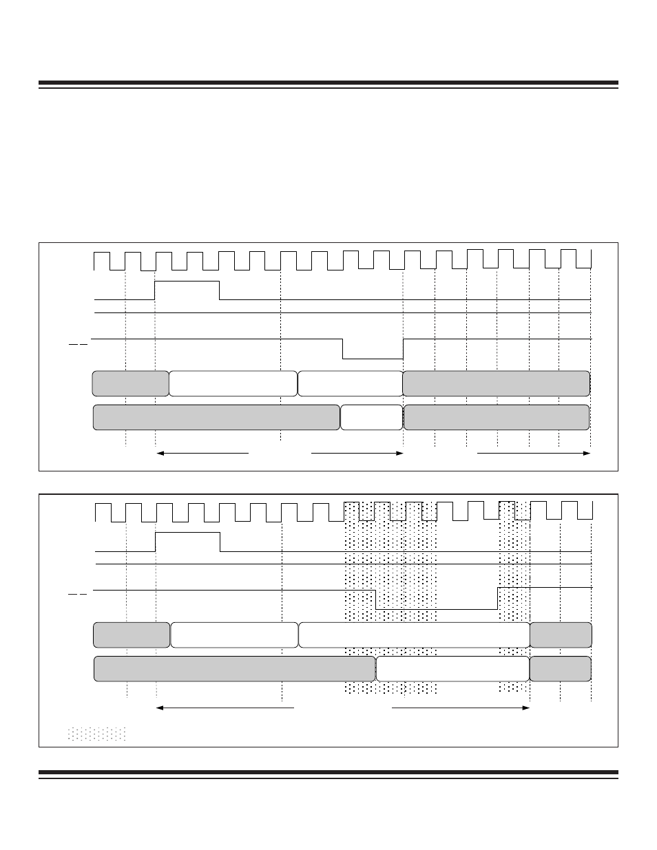
Page Mode 1 Data Memory Timing–PAGES 1:0 = 10b (Four Cycles)
Figure 6-13 shows execution of the MOVX instruction from internal program memory with stretch value = 0 assigned (MD2:0 = 000b).
Note that the internal memory cycles consist of one system clock while the external memory cycles consist of four system clocks (page
hit) or eight system clocks (page miss).
Figure 6-14 illustrates the same MOVX instruction with a default stretch value (MD2:0 = 001b). The stretch cycle (four system clocks)
is distributed as follows: one system clock added for address setup, two system clocks being added to the RD or WR pulse duration,
and one system clock added for address/data hold. For subsequent stretch values of 2 or 3, the full stretch cycle is added to the dura-
tion of the RD or WR pulse.
Ultra-High-Speed Flash
Microcontroller User’s Guide
SYSCLK
ALE
PSEN
PORT2
PORT0
WR/RD
MOVX MSB
MOVX LSB
DATA
MOVX
INST
INSTRUCTIONS
MOVX DATA ACCESS
(PAGE MISS)
SYSCLK
ALE
PSEN
PORT2
PORT0
WR/RD
MOVX
INST
INST
INST
MOVX DATA ACCESS
(PAGE MISS + 1 STRETCH CYCLE)
MOVX MSB
MOVX LSB
MOVX DATA
= STRETCH CYCLE
Figure 6-14. Four-Cycle Page Mode 1: MOVX (Three Cycles)
Figure 6-13. Four-Cycle Page Mode 1: MOVX (Two Cycles)
Maxim Integrated
