Option control register byte, Option control register byte -5, Figure 6-1. memory map for the ds89c420/430 -5 – Maxim Integrated Ultra-High-Speed Flash Microcontroller User Manual
Page 72
6-5
Option Control Register Byte
User-selectable options are present that must be set before beginning software execution. The option control register uses flash bits,
rather than SFRs, and is individually erasable and programmable as a byte-wide register. Bit 3 of this register is defined as the watch-
dog POR default. Setting this bit to 1 disables the watchdog reset function on power-up, and clearing this bit to 0 enables the watchdog
reset function automatically. Other bits of this register are undefined and are at logic 1 when read. The value of this register can be read
at address FCh in parallel programming mode or by executing the verify option control register instruction in ROM Loader mode.
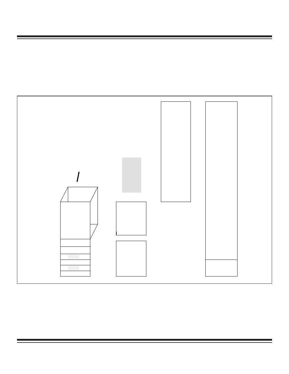
External
Data
Memory
8kB x 8
Flash
Memory
(Program)
1kB x 8
SRAM
Data OR
prog mem
addr from
400–7FF
128 Bytes
Indirect
Addressing
Bit Addressable
Bank 3
Bank 2
Bank 1
Bank 0
00
1F
20
2F
7F
80
128 Bytes SFR
FF
0000
1FFF
2000
3FFF
INTERNAL
MEMORY
03FF
0000
FFFF
FFFF
4000
0000
0000
03FF
External
Program
Memory
INTERNAL
REGISTERS
8kB x 8
Flash
Memory
(Program)
SCRATCH
PAD
Note: The hatched areas shown on the internal and external
memory are disabled on power-up (Default)
Non-usable if
Internal SRAM
is activated
Figure 6-1. Memory Map for the DS89C420/430
Ultra-High-Speed Flash
Microcontroller User’s Guide
Maxim Integrated