Slave address register 0 (sa, Slave address register 1 (sa, Port 3 (p3) – Maxim Integrated Ultra-High-Speed Flash Microcontroller User Manual
Page 33: Slave address register 0 (saddr0) -25, Slave address register 1 (saddr1) -25, Port 3 (p3) -25, Slave address register 1 (saddr1), Slave address register 0 (saddr0)
4-25
ET0
Bit 1
EX0
Bit 0
Enable Timer 0 Interrupt. This bit controls the masking of the Timer 0 interrupt.
0 = Disable all Timer 0 interrupts.
1 = Enable all interrupt requests generated by the TF0 flag (TCON.5).
Enable External Interrupt 0. This bit controls the masking of external interrupt 0.
0 = Disable external interrupt 0.
1 = Enable all interrupt requests generated by the INT0 pin.
SADDR0.7–0
Bits 7–0
Slave Address Register 0. This register is programmed with the given or broadcast address
assigned to serial port 0.
SADDR1.7–0
Bits 7–0
Slave Address Register 1. This register is programmed with the given or broadcast address
assigned to serial port 1.
P3.7–0
Bits 7–0
RD
Bit 7
WR
Bit 6
T1
Bit 5
T0
Bit 4
INT1
Bit 3
Purpose I/O Port 3. This register functions as a general-purpose I/O port. In addition, all the pins
have an alternative function listed below. Each of the functions is controlled by several other SFRs.
The associated port 3 latch bit must contain a logic 1 before the pin can be used in its alternate
function capacity.
External Data Memory Read Strobe. This pin provides an active-low read strobe to an external
memory device.
External Data Memory Write Strobe. This pin provides an active-low write strobe to an external
memory device.
Timer/Counter External Input. A 1-to-0 transition on this pin increments Timer 1.
Counter External Input. A 1-to-0 transition on this pin increments Timer 0.
External Interrupt 1. A falling edge/low level on this pin causes an external interrupt 1 if enabled.
R = Unrestricted read, W = Unrestricted write, -n = Value after reset
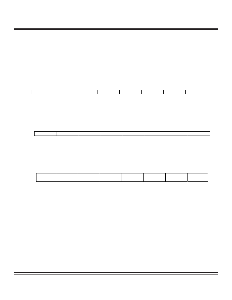
Port 3 (P3)
7
6
5
4
3
2
1
0
SFR B0h
P3.7
RD
P3.6
WR
P3.5
T1
P3.4
T0
P3.3
INT1
P3.2
INT0
P3.1
TXD0
P3.0
RXD0
RW-1
RW-1
RW-1
RW-1
RW-1
RW-1
RW-1
RW-1
R = Unrestricted read, W = Unrestricted write, -n = Value after reset
Slave Address Register 1 (SADDR1)
7
6
5
4
3
2
1
0
SFR AAh
SADDR1.7
SADDR1.6
SADDR1.5
SADDR1.4
SADDR1.3
SADDR1.2
SADDR1.1
SADDR1.0
RW-0
RW-0
RW-0
RW-0
RW-0
RW-0
RW-0
RW-0
R = Unrestricted read, W = Unrestricted write, -n = Value after reset
Slave Address Register 0 (SADDR0)
7
6
5
4
3
2
1
0
SFR A9h
SADDR0.7
SADDR0.6
SADDR0.5
SADDR0.4
SADDR0.3
SADDR0.2
SADDR0.1
SADDR0.0
RW-0
RW-0
RW-0
RW-0
RW-0
RW-0
RW-0
RW-0
Ultra-High-Speed Flash
Microcontroller User’s Guide
Maxim Integrated