Timer 2 lsb (tl2), Timer 2 msb (th2), Program status word (psw) – Maxim Integrated Ultra-High-Speed Flash Microcontroller User Manual
Page 43: Timer 2 lsb (tl2) -35, Timer 2 msb (th2) -35, Program status word (psw) -35, Table 4-19. register bank addresses -35, Table 4-19. register bank addresses
4-35
TL2.7–0
Bits 7–0
Timer 2 LSB. This register contains the least significant byte of Timer 2.
TH2.7–0
Bits 7–0
Timer 2 MSB. This register contains the most significant byte of Timer 2.
CY
Bit 7
AC
Bit 6
F0
Bit 5
RS1, RS0
Bits 4-3
Carry Flag. This bit is set if the last arithmetic operation resulted in a carry (during addition) or a
borrow (during subtraction). Otherwise, it is cleared to 0 by all arithmetic operations.
Auxiliary Carry Flag. This bit is set to 1 if the last arithmetic operation resulted in a carry into (dur-
ing addition) or a borrow (during subtraction) from the high-order nibble. Otherwise, it is cleared to
0 by all arithmetic operations.
User Flag 0. This is a bit-addressable, general-purpose flag for software control.
Register Bank Select 1–0. These bits select which register bank is addressed during register
accesses.
R = Unrestricted read, W = Unrestricted write, -n = Value after reset
Program Status Word (PSW)
7
6
5
4
3
2
1
0
SFR D0h
CY
AC
F0
RS1
RS0
OV
F1
PARITY
RW-0
RW-0
RW-0
RW-0
RW-0
RW-0
RW-0
RW-0
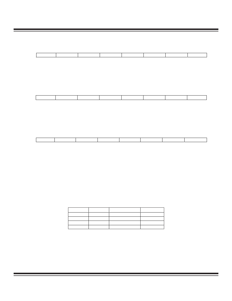
Table 4-19. Register Bank Addresses
RS1
RS0
REGISTER BANK
ADDRESS
0
0
0
00h – 07h
0
1
1
08h – 0Fh
1
0
2
10h – 17h
1
1
3
18h – 1Fh
OV
Bit 2
F1
Bit 1
PARITY
Bit 0
Overflow Flag. This bit is set to 1 if the last arithmetic operation resulted in a carry (addition), bor-
row (subtraction), or overflow (multiplication or division). Otherwise it is cleared to 0 by all arith-
metic operations.
User Flag 1. This is a bit-addressable, general-purpose flag for software control.
Parity Flag. This bit is set to 1 if the module-2 sum of the 8 bits of the accumulator is 1 (odd parity)
and cleared to 0 on even parity.
R = Unrestricted read, W = Unrestricted write, -n = Value after reset
Timer 2 MSB (TH2)
7
6
5
4
3
2
1
0
SFR CDh
TH2.7
TH2.6
TH2.5
TH2.4
TH2.3
TH2.2
TH2.1
TH2.0
RW-0
RW-0
RW-0
RW-0
RW-0
RW-0
RW-0
RW-0
R = Unrestricted read, W = Unrestricted write, -n = Value after reset
Timer 2 LSB (TL2)
7
6
5
4
3
2
1
0
SFR CCh
TL2.7
TL2.6
TL2.5
TL2.4
TL2.3
TL2.2
TL2.1
TL2.0
RW-0
RW-0
RW-0
RW-0
RW-0
RW-0
RW-0
RW-0
Ultra-High-Speed Flash
Microcontroller User’s Guide
Maxim Integrated