Maxim Integrated Ultra-High-Speed Flash Microcontroller User Manual
Page 56
5-9
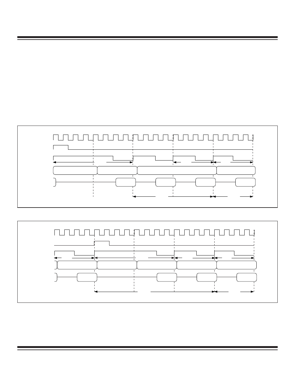
Page Mode 1 External Timing—Pages 1:0 = 10b (Four Cycles)
The page mode 1 external bus structure multiplexes port 2 to provide the address MSB and LSB. Data transactions occur exclusive-
ly on port 0. ALE is used to latch the address MSB only when needed, and PSEN serves as the enable for external program memory.
Page mode 1 must be initiated by internal code memory. To invoke 4-cycle page mode 1 operation, the PAGES1:0 bits must be set to
10b, followed by the setting of the PAGEE bit. In the four-cycle page mode 1 configuration, a page-hit memory cycle is four system
clocks in length, while the page-miss memory cycle requires eight system clocks.
Figure 5-9 shows the fetch of the DA A instruction (1 byte, two cycles) during a page-miss memory cycle as would occur when a page
boundary is crossed. Like nonpage mode operation, a “dummy” or stall cycle must then be inserted for the single-byte DA A instruc-
tion, since it requires two cycles of execution time. After stalling for one cycle, the real fetch of the RRC A instruction takes place.
Figure 5-10 illustrates the fetch of the DA A instruction as the last byte of a 256-byte page. In this case, the stall cycle needed in exe-
cuting the DA A instruction coincides with a page-miss memory cycle instead of a page hit (as in Figure 5-9).
MISS
STALL
SYSCLK
ALE
PSEN
PORT 2
PORT 0
DA A
D4
13
13
RRC A
HIT
HIT
HIT
LSB ADDRESS
LSB ADDRESS
LSB ADDRESS
LSB ADDRESS
MSB ADDRESS
Figure 5-10. Nonpage Mode: DA A – (Page Miss) – RRC A
SYSCLK
ALE
PSEN
PORT 2
PORT 0
MSB ADDRESS
DA A
RRC A
D4
13
13
LSB ADDRESS
LSB ADDRESS
LSB ADDRESS
MISS
HIT
HIT
STALL
Figure 5-9. Four-Cycle Page Mode 1: (Page Miss) – DA A – RRC A
Ultra-High-Speed Flash
Microcontroller User’s Guide
Maxim Integrated