Maxim Integrated Ultra-High-Speed Flash Microcontroller User Manual
Page 59

5-12
Ultra-High-Speed Flash
Microcontroller User’s Guide
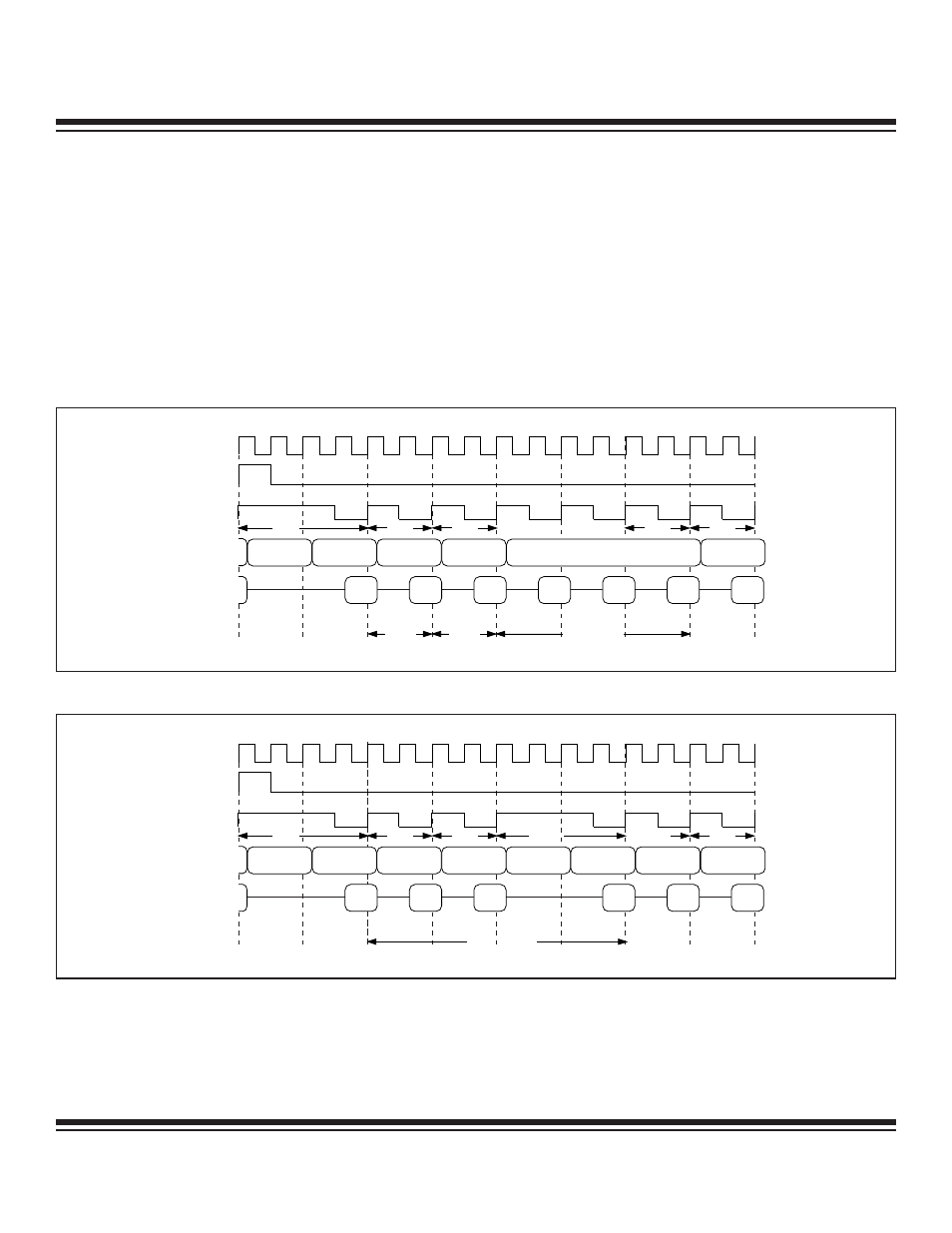
Page Mode 1 External Timing—Pages 1:0 = 01b (Two Cycles)
The page mode 1 external bus structure multiplexes port 2 to provide the address MSB and LSB. Data transactions occur exclusive-
ly on port 0. ALE is used to latch the Address MSB only when needed, and PSEN serves as the enable for external program memory.
To invoke two-cycle page mode 1 operation, the PAGES1:0 bits must be set to 01b, followed by the setting of the PAGEE bit. In the
two-cycle page mode 1 configuration, a page-hit memory cycle is two system clocks in length, while the page-miss memory cycle
requires four system clocks.
Figure 5-15 shows the fetch of the CLR C instruction (1 byte, one cycle) during a page-miss memory cycle, followed by the fetch of
the RRC A instruction (1 byte, one cycle) during a page-hit memory cycle. Since the next instruction, XCH A, @R0 (1 byte, three cycles),
requires three memory cycles to execute, two stall cycles must be inserted for it to complete prior to the next instruction being read.
Figure 5-16 illustrates the LJMP (3 bytes, three cycles) instruction, whose destination address is on a different 256-byte page than the
LJMP instruction, thus resulting in a page-miss memory cycle.
SYSCLK
ALE
PSEN
PORT 2
PORT 0
02
50
00
MISS
HIT
MISS
LJMP ADDR16
HIT
HIT
HIT
LSB
MSB
LSB
LSB
LSB
LSB
MSB
LSB
Figure 5-16. Two-Cycle Page Mode 1: (Page Miss) – LJMP ADDR16 – (Page Miss)
SYSCLK
ALE
PSEN
PORT 2
PORT 0
C3
13
C6
MISS
HIT
STALL
STALL
XCH A, @R0
HIT
HIT
HIT
CLR C
RRC A
LSB
MSB
LSB
LSB
LSB
LSB ADDRESS
Figure 5-15. Two-Cycle Page Mode 1: (Page Miss) – CLR C – RRC A – XCH A, @R0
Maxim Integrated
