Page mode 2 bus structure – Maxim Integrated Ultra-High-Speed Flash Microcontroller User Manual
Page 78
6-11
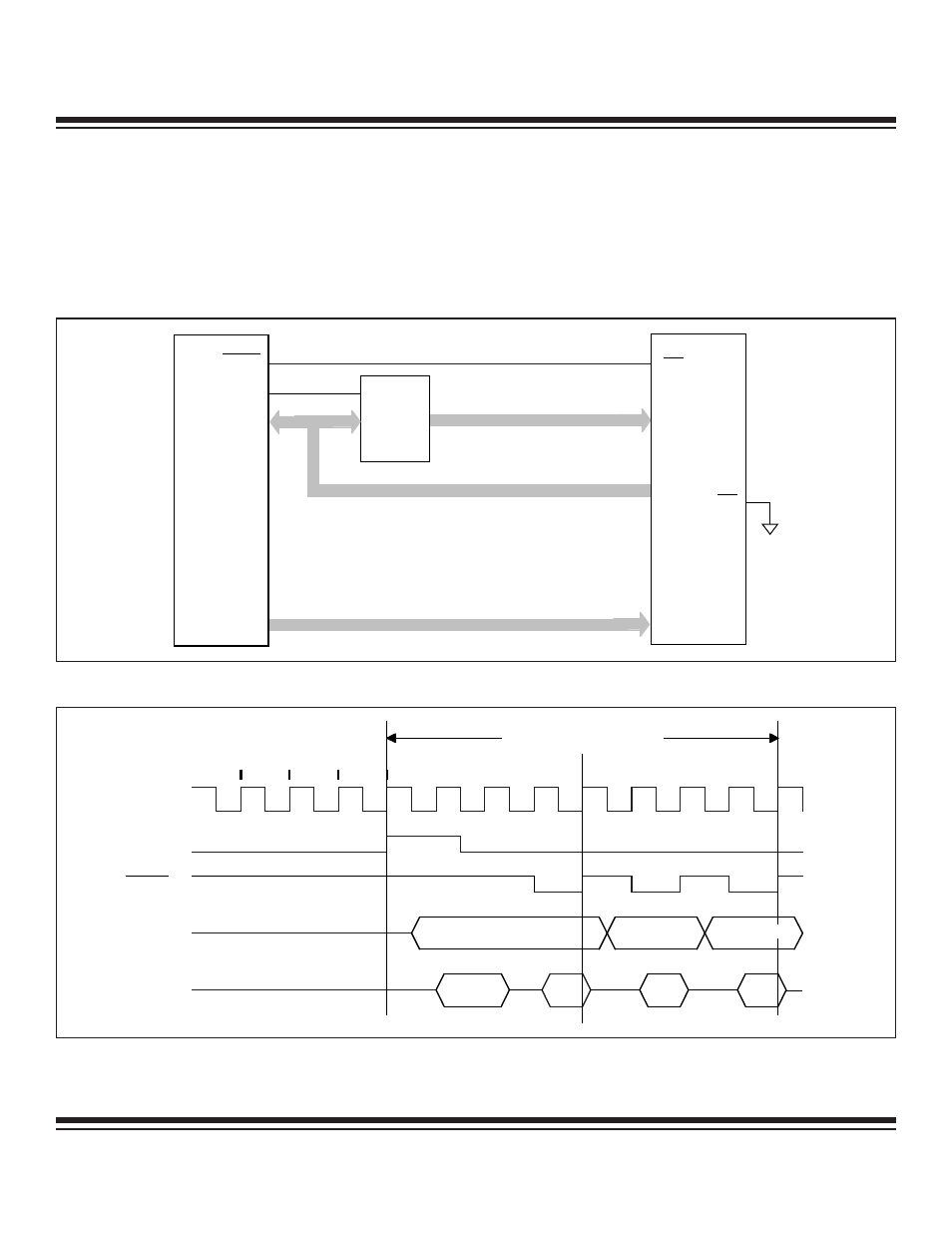
Page Mode 2 Bus Structure
The page mode 2 external bus structure multiplexes the most significant address byte with data on P2 and uses P0 for the least sig-
nificant address byte. An illustration of this memory interface is provided in Figure 6-6.
This bus structure speeds up external code fetches only. Aside from the different functions of P0 and P2 when operating in page mode
2, the external memory accesses are equal in duration and timing to those made in the nonpage mode. Figure 6-7 illustrates memory
cycles for the page mode 2 bus structure.
Internal Memory Cycles
C2
C3 C4 C1 C2 C1 C2
XTAL1
ALE
Port 0
Port 2
PSEN
C1
Ext Code Fetches
Page Miss
Page Hit
Page Hit
Data
Data
LSB Add
LSB Add
LSB Add
Data
MSB Add
Figure 6-7. Page Mode 2 External Code Fetch Cycle (CD1:0 = 10b)
PSEN
ALE
CK
74F373
LATCH
MSB ADDRESS
DATA BUS
LSB ADDRESS
PORT 0
(8)
(8)
64kB X 8
MEMORY
(8)
OE
CE
PORT 2
DS89C4x0
Figure 6-6. Program Memory Interconnect (Page Mode 2)
Ultra-High-Speed Flash
Microcontroller User’s Guide
Maxim Integrated
- DS80C390 (58 pages)
- DS5001FP (26 pages)
- MAX1416 (14 pages)
- MAX5865 (18 pages)
- DS33Z41 (167 pages)
- MAX1202 (7 pages)
- USBTO232 (31 pages)
- HFAN-09.5.0: Pattern Creator/Converter Software (8 pages)
- MAX-IDE MAXQ Microcontrollers (11 pages)
- MAX6876 Power-Supply Tracker/Sequencer (6 pages)
- MAX6877 Power-Supply Tracker/Sequencer (3 pages)
- 78Q8430 ARM9(920T) Linux Driver Diagnostic Guide (19 pages)
- 78Q8430 Software Driver (54 pages)
- 78Q8430 ST 5100/OS-20 with NexGen TCP/IP Stack (28 pages)
- 6612_OMU_S2_URT_V1_13 (56 pages)
- 6612_OMU_S2+2_URT_V1_14 (58 pages)
- 71M6511 Power Meter IC Family Software (137 pages)
- 71M65xx ADM51 ICE Safety Notice (2 pages)
- 71M6511 2-Layer Demo Board (2 pages)
- 71M6511 4-Layer Demo Board (2 pages)
- 78Q8430 Linux Driver ARM Platform (22 pages)
- 71M6513 Demo Board (2 pages)
- 71M6521DE Energy Meter IC Family Software (138 pages)
- 71M6521 Demo Board (2 pages)
- 71M6531 Demo Board (2 pages)
- 71M6531 Energy Meter IC Family Software (116 pages)
- 71M6533 Demo Board (2 pages)
- 71M6534H Demo Board (2 pages)
- 71M6515H Demo Board (2 pages)
- 73S1209F Evaluation Board (2 pages)
- 73S12xxF (38 pages)
- 73S12xxF Software (93 pages)
- 73S1210F Evaluation Board Lite (2 pages)
- 73S1210F Evaluation Board (2 pages)
- 73S1210F Multi-SAM Evaluation Board Lite (2 pages)
- 73S12xxF USB-CCID Linux DFU Host Application (8 pages)
- 73S1215F Device Firmware Upgrade Host Driver/Application (10 pages)
- 73S12xxF USB-CCID Host GUI (22 pages)
- 73S1215F Windows XP 32 USB CCID and DFU Drivers (15 pages)
- 73S1215F CCID USB Linux Driver (16 pages)
- 73S1215F Evaluation Board (2 pages)
- 73S1215F Evaluation Board Lite (2 pages)
- 73S1217F Evaluation Board (2 pages)
- 73S1217F Evaluation Board Lite (2 pages)
- MAXQ Family (216 pages)