Power management register (pmr), Power management register (pmr) -30, Table 4-16. on-chip rom address -30 – Maxim Integrated Ultra-High-Speed Flash Microcontroller User Manual
Page 38: Table 4-16. on-chip rom address
4-30
Ultra-High-Speed Flash
Microcontroller User’s Guide
RMS2–0
Bits 2–0
ROM Memory Size Select 2-0. This register is used to select the maximum on-chip decoded
address. Care must be taken that the memory location of the current program counter is valid both
before and after modification. These bits can only be modified using a timed-access procedure. The
EA pin overrides the function of these bits when asserted, forcing the device to access external pro-
gram memory only. Configuring this register to a setting that exceeds the maximum amount of inter-
nal memory can corrupt device operation. These bits default on reset to the maximum amount of
internal program memory (i.e., 16k for DS89C420).
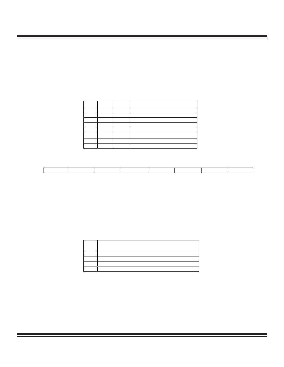
Table 4-16. On-Chip ROM Address
RMS2
RMS1
RMS0
MAXIMUM ON-CHIP ROM ADDRESS
0
0
0
0kB/Disable on-chip ROM
0
0
1
1kB/03FFh
0
1
0
2kB/07FFh
0
1
1
4kB/0FFFh
1
0
0
8kB/1FFFh
1
0
1
16kB/3FFFh (DS89C420/430 default)
1
1
0
32kB/7FFFh (DS89C440 default)
1
1
1
64kB/FFFFh (DS89C450 default)
CD1,
CD0
CLOCK FUNCTION
00
Crystal multiplier (4X or 2X mode as determined by PMR.3)
01
Reserved (forced into divide-by-1 mode if set)
10
Divide-by-1 (default state)
11
Divide-by-1024
R = Unrestricted read, W = Unrestricted write, -n = Value after reset, * = See description
Power Management Register (PMR)
7
6
5
4
3
2
1
0
SFR C4h
CD1
CD0
SWB
CTM
4X/2X
ALEON
DME1
DME0
RW*-1
RW*-0
RW-0
RW*-0
RW*-0
RW-0
RW-0
RW-0
CD1, CD0
Bits 7, 6
Clock Divide Control 1-0. These bits select the number of crystal oscillator clocks required to gen-
erate one machine cycle. Switching between modes requires a transition through the default
divide-by-1 mode (CD1, CD0 = 10b). Attempts to perform an invalid transition are ignored. For
example, going from the crystal multiplier 2X mode to the divide-by-1024 mode would require first
switching from the 2X crystal multiplier mode to the divide-by-1 mode, followed by the switch from
the divide-by-1 to the divide-by-1024 mode. These bits cannot be modified when running from the
internal ring oscillator (RGMD = 1). The divide-by-1024 setting (CD1,CD0 = 11b) cannot be selected
when switchback is enabled (SWB = 1) and a switchback source (serial port or external interrupt)
is active.
The setting of these bits affects timer and serial port operation. Tables located in the SFR decription for
CKCON (8Eh) detail the respective operational dependencies on these bits.
Maxim Integrated