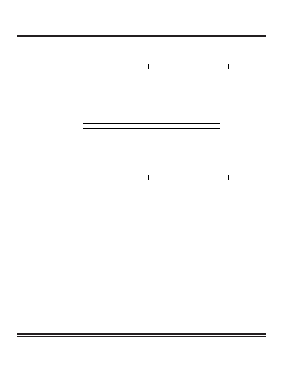
Port 2 (p2), Interrupt enable (ie), Port 2 (p2) -24 – Maxim Integrated Ultra-High-Speed Flash Microcontroller User Manual
Page 32: Interrupt enable (ie) -24, Table 4-12. port 2 functions -24, Table 4-12. port 2 functions

4-24
Ultra-High-Speed Flash
Microcontroller User’s Guide
P2.7–0
Bits 7–0
Port 2. This port functions according to the table below where PAGEE = ACON.7 and PAGES =
ACON.6-5.
EA
Bit 7
ES1
Bit 6
ET2
Bit 5
ES0
Bit 4
ET1
Bit 3
EX1
Bit 2
Global Interrupt Enable. This bit controls the global masking of all interrupts except power-fail
interrupt, which is enabled by the EPFI bit (WDCON.5).
0 = Disable all interrupt sources. This bit overrides individual interrupt mask settings.
1 = Enable all individual interrupt masks. Individual interrupts occur if enabled.
Enable Serial Port 1 Interrupt. This bit controls the masking of the serial port 1 interrupt.
0 = Disable all serial port 1 interrupts.
1 = Enable interrupt requests generated by the RI_1 (SCON1.0) or TI_1 (SCON1.1) flags.
Enable Timer 2 Interrupt. This bit controls the masking of the Timer 2 interrupt.
0 = Disable all Timer 2 interrupts.
1 = Enable interrupt requests generated by the TF2 flag (T2CON.7).
Enable Serial Port 0 Interrupt. This bit controls the masking of the serial port 0 interrupt.
0 = Disable all serial port 0 interrupts.
1 = Enable interrupt requests generated by the RI_0 (SCON0.0) or TI_0 (SCON0.1) flags.
Enable Timer 1 Interrupt. This bit controls the masking of the Timer 1 interrupt.
0 = Disable all Timer 1 interrupts.
1 = Enable all interrupt requests generated by the TF1 flag (TCON.7).
Enable External Interrupt 1. This bit controls the masking of external interrupt 1.
0 = Disable external interrupt 1.
1 = Enable all interrupt requests generated by the INT0 pin.
Writing a 1 to an SFR bit configures the associated port pin as an input. All read operations, with
the exception of read-modify-write instructions, leave the port latch unchanged. During external
memory addressing and data memory write cycles, the port has high and low drive capability.
During external memory data read cycles, the port is held in a high-impedance state.
Table 4-12. Port 2 Functions
PAGEE
PAGES
PORT2 FUNCTION
0
XX
General-Purpose I/0 (code execution < ROMSIZE.2-0)
0
XX
Address MSB (code execution > ROMSIZE.2-0)
1
00, 01, 10
Multiplexed Address MSB/LSB
1
11
Multiplexed Address MSB/Data
R = Unrestricted read, W = Unrestricted write, -n = Value after reset
Interrupt Enable (IE)
7
6
5
4
3
2
1
0
SFR A8h
EA
ES1
ET2
ES0
ET1
EX1
ET0
EX0
RW-0
RW-0
RW-0
RW-0
RW-0
RW-0
RW-0
RW-0
R = Unrestricted read, W = Unrestricted write, -n = Value after reset
Port 2 (P2)
7
6
5
4
3
2
1
0
SFR A0h
P2.7
P2.6
P2.5
P2.4
P2.3
P2.2
P2.1
P2.0
RW-1
RW-1
RW-1
RW-1
RW-1
RW-1
RW-1
RW-1
Maxim Integrated
