Interrupt priority 0 (ip0), Slave address mask enable re, Interrupt priority 0 (ip0) -27 – Maxim Integrated Ultra-High-Speed Flash Microcontroller User Manual
Page 35: Slave address mask enable register 0 (saden0) -27, Slave address mask enable register 0 (saden0)
4-27
IP07.0
Bit 7
LPS1
Bit 6
LPT2
Bit 5
LPS0
Bit 4
LPT1
Bit 3
LPX1
Bit 2
LPT0
Bit 1
LPX0
Bit 0
Reserved. Read data is 1.
Least Significant Priority Select Bit for Serial Port 1 Interrupt. LPS1 is the least significant bit
of the bit pair MPS1 (IP1.6), LPS1 that designates priority level for the serial port 1 interrupt.
Least Significant Priority Select Bit for Timer 2 Interrupt. LPT2 is the least significant bit of the
bit pair MPT2 (IP1.5), LPT2 that designates priority level for the Timer 2 interrupt.
Least Significant Priority Select Bit for Serial Port 0 Interrupt. MPS0 is the least significant bit
of the bit pair MPS0 (IP1.4), LPS0 that designates priority level for the serial port 0 interrupt.
Least Significant Priority Select Bit for Timer 1 Interrupt. MPT1 is the least significant bit of the
bit pair MPT1 (IP1.3), LPT1 that designates priority level for the Timer 1 interrupt.
Least Significant Priority Select Bit for External Interrupt 1. MPX1 is the least significant bit of
the bit pair MPX1 (IP1.2), LPX1 that designates priority level for external interrupt 1.
Least Significant Priority Select Bit for Timer 0 Interrupt. MPT0 is the least significant bit of the
bit pair MPT0 (IP1.1), LPT0 that designates priority level for the Timer 0 interrupt.
Least Significant Priority Select Bit for External Interrupt 0. MPX0 is the least significant bit of
the bit pair MPX0 (IP1.0), LPX0 that designates priority level for external interrupt 0.
R = Unrestricted read, W = Unrestricted write, -n = Value after reset
Slave Address Mask Enable Register 0 (SADEN0)
Table 4-14. Least Significant Priority Select Bit Levels
MP (IP1.X)
LP (IP0.X)
PRIORITY LEVEL
0
0
0 (natural priority)
0
1
1
1
0
2
1
1
3 (high priority)
7
6
5
4
3
2
1
0
SFR B9h
SADEN0.7
SADEN0.6
SADEN0.5
SADEN0.4
SADEN0.3
SADEN0.2
SADEN0.1
SADEN0.0
RW-0
RW-0
RW-0
RW-0
RW-0
RW-0
RW-0
RW-0
SADEN0.7–0
Bits 7–0
Slave Address Mask Enable Register 0. This register functions as a mask when comparing ser-
ial port 0 addresses for automatic address recognition. When a bit in this register is set, the corre-
sponding bit location in the SADDR0 register is exactly compared with the incoming serial port 0
data to determine if a receiver interrupt should be generated. When a bit in this register is cleared,
the corresponding bit in the SADDR0 register becomes a “don’t care” and is not compared against
the incoming data. All incoming data generates a receiver interrupt when this register is cleared.
R = Unrestricted read, W = Unrestricted write, -n = Value after reset
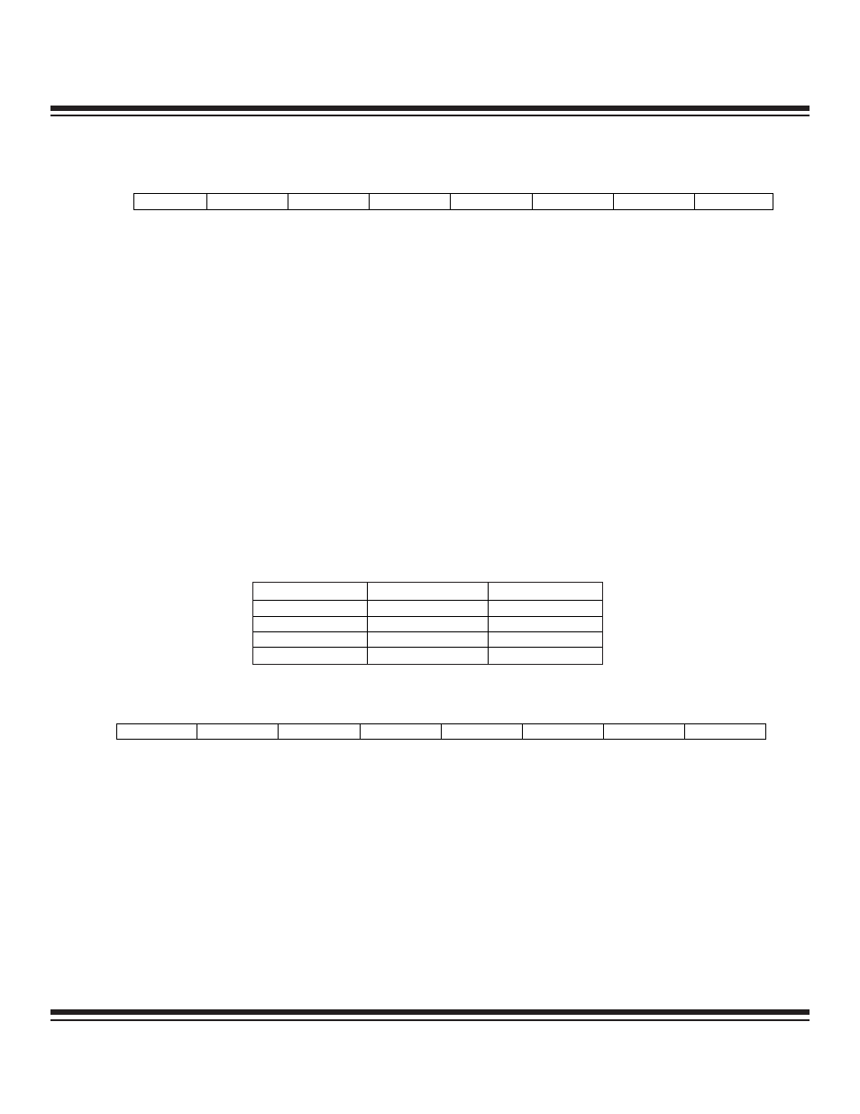
Interrupt Priority 0 (IP0)
7
6
5
4
3
2
1
0
SFR B8h
—
LPS1
LPT2
LPS0
LPT1
LPX1
LPT0
LPX0
R-1
RW-0
RW-0
RW-0
RW-0
RW-0
RW-0
RW-0
Ultra-High-Speed Flash
Microcontroller User’s Guide
Maxim Integrated