Program memory interface—pag, Table 6-3. page mode select – Maxim Integrated Ultra-High-Speed Flash Microcontroller User Manual
Page 75
6-8
Ultra-High-Speed Flash
Microcontroller User’s Guide
Program Memory Interface—Page Modes
Page mode retains the basic external circuitry requirements as the original 8051 external memory interface, but modifies the
address/data roles of P0 and P2 in order to achieve the most efficient single-cycle external operation possible. The functions of ALE
and PSEN are also altered to support page mode operation.
Page mode is enabled by setting the PAGEE (ACON.7) bit to a logic 1. Clearing the PAGEE bit disables the page mode and returns
to the traditional external bus structure of the 8051 (nonpage mode). Page mode is supported in two external bus structures. The page
mode select bits (PAGES1:0) contained in the ACON register determine the external bus structure and the number of system clocks
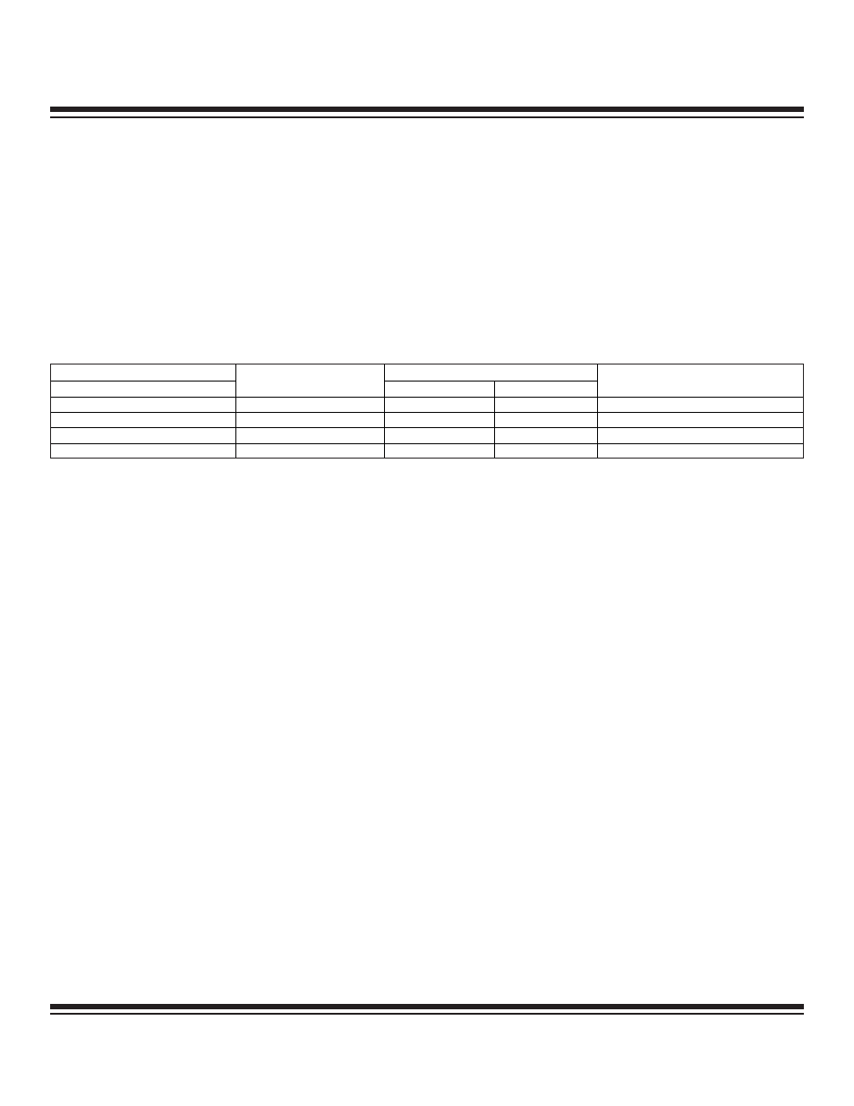
per basic memory cycle. The following table summarizes the four options available through the PAGES bits. The first three selections
all represent the page mode 1 external bus structure, but with different memory cycle timings. The last configuration (PAGES = 11b)
selects the page mode 2 bus structure.
EXTERNAL ADDRESSING
CLOCKS PER MEMORY CYCLE
MODE
PAGES1:PAGES0
PAGE HIT
PAGE MISS
EXTERNAL BUS STRUCTURE
Page mode 1 (1 cycle)
00
1
2
PAGE MODE 1
Page mode 1 (2 cycle)
01
2
4
PAGE MODE 1
Page mode 1 (4 cycle)
10
4
8
PAGE MODE 1
Page mode 2
11
2*
4
PAGE MODE 2
Note: External data memory accesses always require four clock cycles, regardless of page hit or page miss.
Table 6-3. Page Mode Select
PAGE MODE 1:
P0: Primary data bus.
P2: Primary address bus, multiplexing the upper byte and lower byte of address.
PAGE MODE 2:
P0: Lower address byte.
P2: Upper address byte is multiplexed with the data byte.
In addition to being accessible to the user application code, the page mode enable and select bits can also be modified while in ROM
loader mode. This allows in-system MOVX read/write access to external memory already connected according to the page mode 1 or
page mode 2 bus structure. Since all resets, including the one generated when exiting ROM loader mode, return to the nonpage mode
external bus structure, user application code must always configure the ACON register appropriately before addressing page mode
external memory. Write access to the ACON register requires using the timed access procedure.
Maxim Integrated