External data memory interfa – Maxim Integrated Ultra-High-Speed Flash Microcontroller User Manual
Page 80

6-13
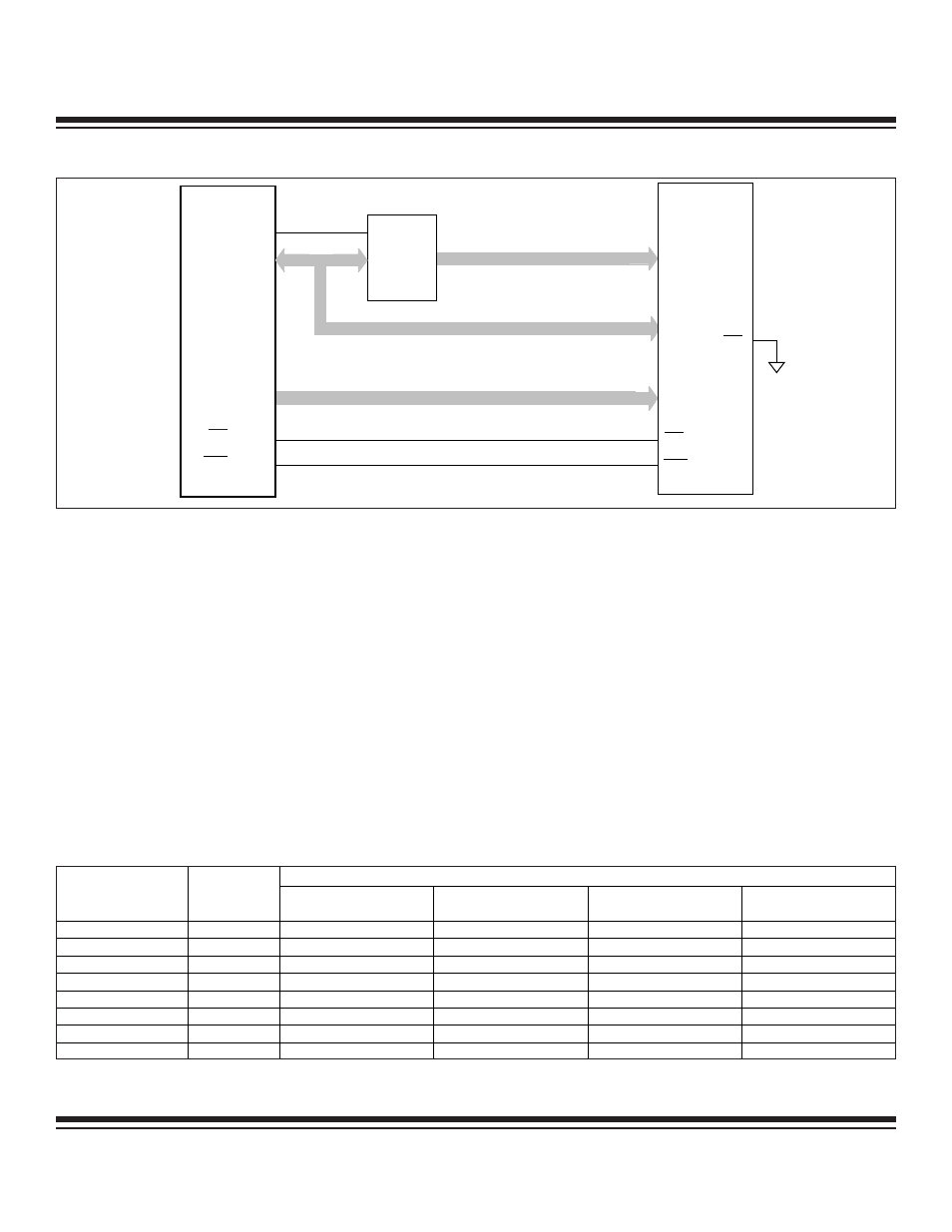
External Data Memory Interface—Page Modes
The ultra-high-speed flash microcontroller allows software to adjust the speed of external data memory access by stretching the mem-
ory bus cycle in page mode operation just like nonpage mode operation. The tables below summarize the stretch values for page mode
1 and page mode 2. The number of stretch cycles added to the external MOVX operation and the control signal pulse width (in terms
of the number of oscillator clocks) are provided. A stretch machine cycle always contains four system clocks, independent of the logic
value of the page mode select bits.
Just like nonpage mode operation, the stretch feature supports eight stretched external data memory access cycles that can be cat-
egorized into three timing groups. When the stretch value is cleared to 000b, there is no stretch on external data memory access and
a MOVX instruction is completed in two basic memory cycles. When the stretch value is set to 001b, 010b, or 011b, the external data
memory access is extended by 1, 2, or 3 stretch machine cycles, respectively. The 001b stretch value does not add four system clocks
to the RD or WR control signals, but instead uses one system clock to create additional address setup and data bus float time and
uses one system clock to create additional address and data hold time. When using very slow RAM and peripherals, a larger stretch
value (4–7) can be selected. In this stretch category, one stretch machine cycle (four system clocks) is used to stretch the ALE pulse
width, one stretch machine cycle is used to create additional setup and one stretch machine cycle is used to create additional hold
time.
Table 6-5. Page Mode 1—Data Memory Stretch Values 1 Cycle (PAGES 1:0 = 00b)
RD
(P3.7)
ALE
CK
74F373
LATCH
LSB ADDRESS
DATA BUS
MSB ADDRESS
PORT 2
(8)
(8)
64kB X 8
SRAM
(8)
PORT 0
WR
(P3.6)
OE
WE
CE
DS89C4x0
Figure 6-8. Data Memory Interconnect (Nonpage Mode)
RD/WR PULSE WIDTH (IN NUMBER OF OSCILLATOR CLOCKS)
MD2:MD0
(STRETCH VALUE)
STRETCH
CYCLES
4X/2X, CD1, CD0 = 100
4X/2X, CD1, CD0 = 000
4X/2X, CD1, CD0 = X10
4X/2X, CD1, CD0 = X11
000
0
0.25
0.5
1
1024
001
1
0.75
1.5
3
3072
010
2
1.75
3.5
7
7168
011
3
2.75
5.5
11
11264
100
7
3.75
7.5
15
15360
101
8
4.75
9.5
19
19456
110
9
5.75
11.5
23
23552
111
10
6.75
13.5
27
27648
Ultra-High-Speed Flash
Microcontroller User’s Guide
Maxim Integrated
