Maxim Integrated Ultra-High-Speed Flash Microcontroller User Manual
Page 76
6-9
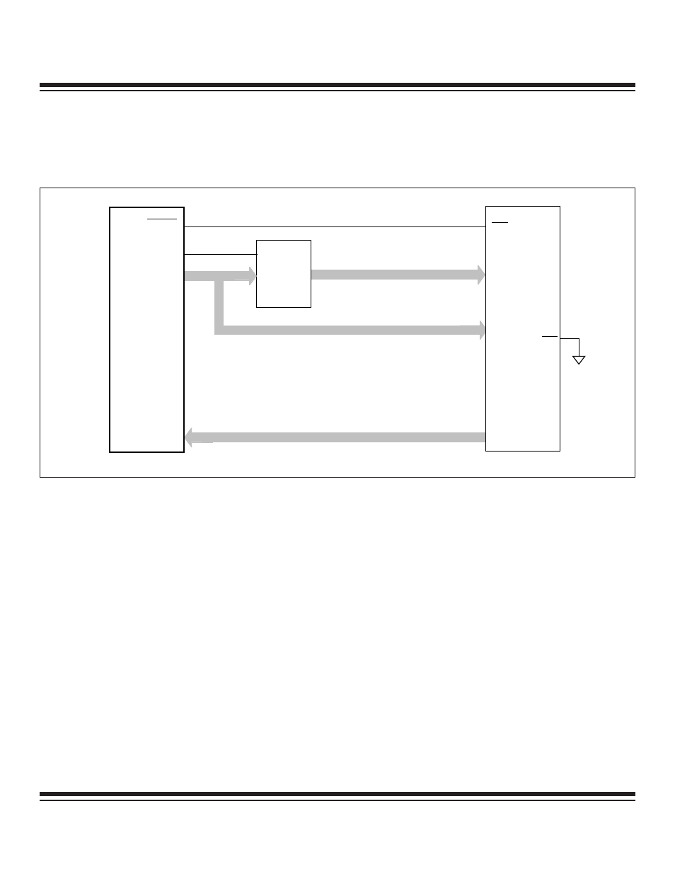
Page Mode 1 Bus Structure
The page mode 1 external bus structure uses P2 as the primary address bus (multiplexing both the most significant byte and least sig-
nificant byte of the address for each external memory cycle), and P0 is used as the primary data bus. This program memory inter-
connect scheme is depicted in Figure 6-4.
During external code fetches, P0 is held in a high-impedance state by the processor. Opcodes are driven by the external memory onto
P0 and latched on the rising edge of PSEN at the end of the external fetch cycle.
•
A page miss occurs when the most significant byte of the subsequent address is different from the last address. The external
memory machine cycle can be 2, 4, or 8 system clocks in length for a page miss.
•
A page hit occurs when the most significant byte of the subsequent address does not change from the last address. The exter-
nal memory machine cycle can be 1, 2, or 4 system clocks in length for a page hit.
During a page hit, P2 drives Addr [7:0] of the 16-bit address while the most significant address byte is held in the external address latch-
es. PSEN, RD, and RD strobe accordingly for the appropriate operation on the P0 data bus. There is no ALE assertion for page hits.
During a page miss, P2 drives the Addr [15:8] of the 16-bit address and holds it for the duration of the first half of the memory cycle
to allow the external address latches to latch the new most significant address byte. ALE is asserted to strobe the external address
latches. During this operation, PSEN, RD, and WR are all held in inactive states and P0 is in a high-impedance state. The following half-
memory cycle is executed as a page-hit cycle and the appropriate operation takes place.
A page-miss can occur at set intervals or during external operations that require a memory access into a page of memory that has not
been accessed during the last external cycle. Generally, the first external memory access causes a page miss. The new page address
is stored internally and is used to detect a page miss for the current external memory cycle.
Note that there are a few exceptions for this mode of operation when PAGES1 and PAGES2 are set to 00b:
• PSEN is asserted for both page hit and page miss for a full clock cycle.
• The execution of external MOVX instruction causes a page miss.
• A page miss occurs when fetching the next external instruction following the execution of an external MOVX instruction.
PSEN
ALE
CK
74F373
LATCH
MSB ADDRESS
LSB ADDRESS
DATA BUS
PORT 0
(8)
(8)
64kB X 8
MEMORY
(8)
OE
CE
PORT 2
DS89C4x0
Figure 6-4 Program Memory Interconnect (Page Mode 1)
Ultra-High-Speed Flash
Microcontroller User’s Guide
Maxim Integrated