Altera Arria 10 Avalon-ST User Manual
Page 99
Signal
Direction
Description
Refer to the appropriate device pinout for correct pin assignment
for more detailed information about these pins. The PCI Express
Card Electromechanical Specification 2.0 specifies this pin
requires 3.3 V. You can drive this 3.3V signal to the
nPERST*
even if the V
VCCPGM
of the bank is not 3.3V if the following 2
conditions are met:
• The input signal meets the V
IH
and V
IL
specification for
LVTTL.
• The input signal meets the overshoot specification for 100°C
operation as defined in the device handbook.
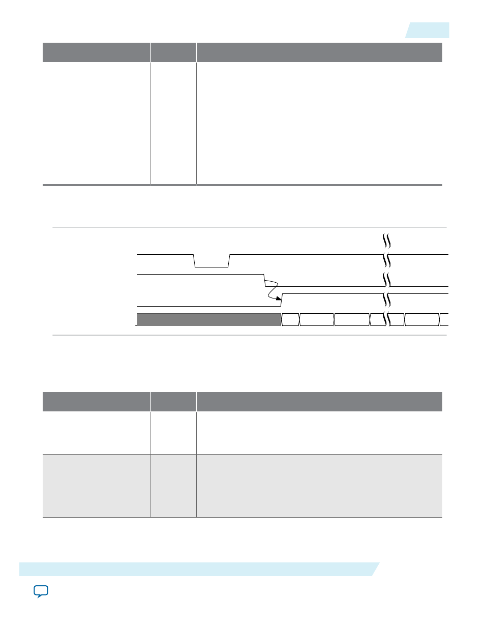
Figure 6-33: Reset and Link Training Timing Relationships
The following figure illustrates the timing relationship between
npor
and the LTSSM L0 state.
npor
IO_POF_Load
PCIe_LinkTraining_Enumeration
dl_ltssm[4:0]
detect detect.active polling.active
L0
Note: To meet the 100 ms system configuration time, you must use the fast passive parallel configuration
scheme with CvP and a 32-bit data width (FPP x32) or use the CvP in autonomous mode.
Table 6-7: Status and Link Training Signals
Signal
Direction
Description
serdes_pll_locked
Output
When asserted, indicates that the PLL that generates the
coreclkout_hip
clock signal is locked. In pipe simulation mode
this signal is always asserted.
pld_core_ready
Input
When asserted, indicates that the Application Layer is ready for
operation and is providing a stable clock to the
pld_clk
input. If
the
coreclkout_hip
Hard IP output clock is sourcing the
pld_
clk
Hard IP input, this input can be connected to the
serdes_
pll_locked
output.
UG-01145_avst
2015.05.04
Reset, Status, and Link Training Signals
6-33
Interfaces and Signal Descriptions
Altera Corporation