Chaining dma control and status registers, Chaining dma control and status registers -9 – Altera Arria 10 Avalon-ST User Manual
Page 209
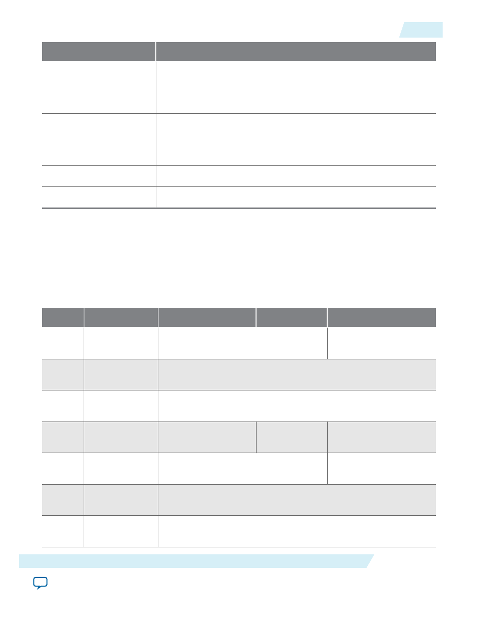
Memory BAR
Mapping
32-bit BAR2
32-bit BAR3
64-bit BAR3:2
Maps to DMA Read and DMA write control and status registers, a
minimum of 256 bytes.
32-bit BAR4
32-bit BAR5
64-bit BAR5:4
Maps to 32 KByte target memory block. Use the rc_slave module to bypass
the chaining DMA.
Expansion ROM BAR
Not implemented by design example; behavior is unpredictable.
I/O Space BAR (any)
Not implemented by design example; behavior is unpredictable.
Chaining DMA Control and Status Registers
The software application programs the chaining DMA control register located in the Endpoint applica‐
tion. The following table describes the control registers which consists of four dwords for the DMA write
and four dwords for the DMA read. The DMA control registers are read/write.
In this table, Addr specifies the Endpoint byte address offset from BAR2 or BAR3.
Table 17-2: Chaining DMA Control Register Definitions
Addr
Register Name
Bits[31:]24
Bit[23:16]
Bit[15:0]
0x0
DMA Wr Cntl DW0
Control Field
Number of descriptors in
descriptor table
0x4
DMA Wr Cntl DW1
Base Address of the Write Descriptor Table (BDT) in the RC Memory–
Upper DWORD
0x8
DMA Wr Cntl DW2
Base Address of the Write Descriptor Table (BDT) in the RC Memory–
Lower DWORD
0xC
DMA Wr Cntl DW3
Reserved
Reserved
RCLAST–Idx of last
descriptor to process
0x10
DMA Rd Cntl DW0
Control Field (described in the next table)
Number of descriptors in
descriptor table
0x14
DMA Rd Cntl DW1
Base Address of the Read Descriptor Table (BDT) in the RC Memory–
Upper DWORD
0x18
DMA Rd Cntl DW2
Base Address of the Read Descriptor Table (BDT) in the RC Memory–
Lower DWORD
UG-01145_avst
2015.05.04
Chaining DMA Control and Status Registers
17-9
Testbench and Design Example
Altera Corporation