Altera Arria 10 Avalon-ST User Manual
Page 211
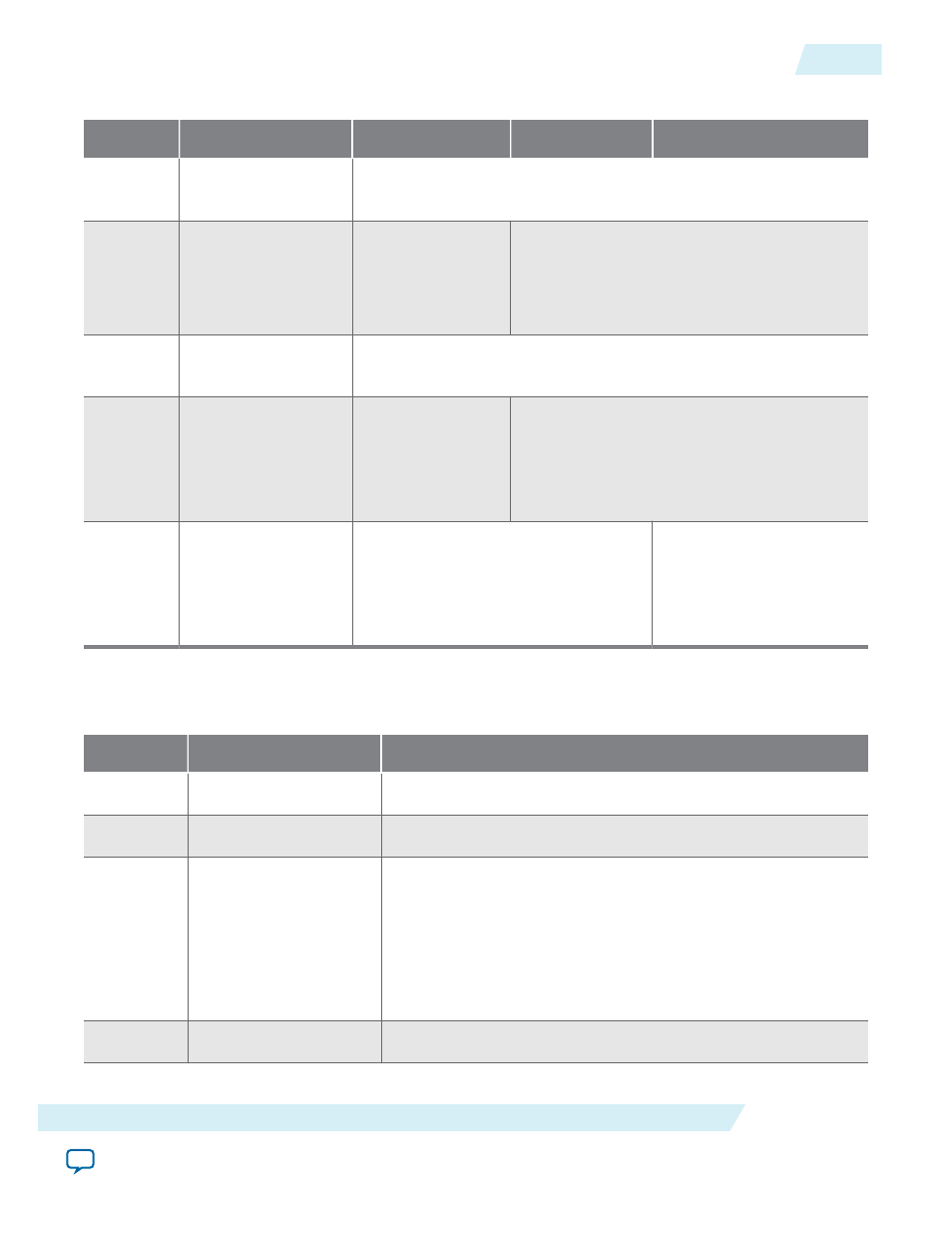
Table 17-4: Chaining DMA Status Register Definitions
Addr
Register Name
Bits[31:24]
Bits[23:16]
Bits[15:0]
0x20
DMA Wr Status Hi
For field definitions refer to Fields in the DMA Write Status High
Register below.
0x24
DMA Wr Status Lo
Target Mem Address
Width
Write DMA Performance Counter. (Clock
cycles from time DMA header programmed
until last descriptor completes, including time
to fetch descriptors.)
0x28
DMA Rd Status Hi
For field definitions refer to Fields in the DMA Read Status High
Register below.
0x2C
DMA Rd Status Lo
Max No. of Tags
Read DMA Performance Counter. The
number of clocks from the time the DMA
header is programmed until the last descriptor
completes, including the time to fetch descrip‐
tors.
0x30
Error Status
Reserved
Error Counter. Number of
bad ECRCs detected by
the Application Layer.
Valid only when ECRC
forwarding is enabled.
The following table describes the fields of the DMA write status register. All of these fields are read only.
Table 17-5: Fields in the DMA Write Status High Register
Bit
Field
Description
[31:28]
CDMA version
Identifies the version of the chaining DMA example design.
[27:24]
Reserved
—
[23:21]
Max payload size
The following encodings are defined:
• 001 128 bytes
• 001 256 bytes
• 010 512 bytes
• 011 1024 bytes
• 100 2048 bytes
[20:17]
Reserved
—
UG-01145_avst
2015.05.04
Chaining DMA Control and Status Registers
17-11
Testbench and Design Example
Altera Corporation