5 hdi08 - dsp-side programmer’s model, Hdi08 – dsp-side programmer’s model -5, Figure 6-1 – Freescale Semiconductor DSP56366 User Manual
Page 99: Hdi08 block diagram -5, 5 hdi08 – dsp-side programmer’s model, Dsp peripheral data bus, Host bus, Core dma data bus
HDI08 – DSP-Side Programmer’s Model
DSP56366 24-Bit Digital Signal Processor User Manual, Rev. 4
Freescale Semiconductor
6-5
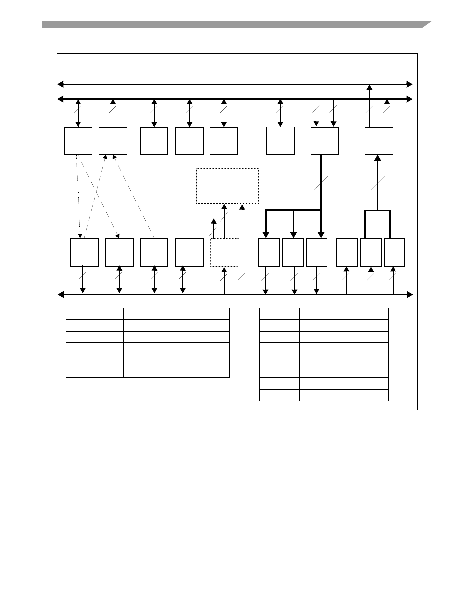
Figure 6-1 HDI08 Block Diagram
6.5
HDI08 – DSP-Side Programmer’s Model
The DSP core threats the HDI08 as a memory-mapped peripheral occupying eight 24-bit words in X data
memory space. The DSP may use the HDI08 as a normal memory-mapped peripheral, employing either
standard polled or interrupt-driven programming techniques. Separate transmit and receive data registers
are double-buffered to allow the DSP and host processor to transfer data efficiently at high speed. Direct
memory mapping allows the DSP core to communicate with the HDI08 registers using standard
instructions and addressing modes. In addition, the MOVEP instruction allows direct data transfers
between the DSP memory and the HDI08 registers or vice-versa. The HOTX and HORX registers may be
serviced by the on-chip DMA controller for data transfers.
RXL
TXM
TXH
8
HPCR
Latch
RXL
IVR
CVR
ICR
24
24
HDDR
HCR
HSR
HDR
24
24
24
24
24
DSP Peripheral Data Bus
8
8
8
8
8
8
5
3
HOST Bus
Address
Comparator
3
8
8
RXM
24
24
HBAR
ISR
8
HOR
HOTX
24
Core DMA Data Bus
24
24
8
RXH
8
HCR
Host Control Register
HSR
Host Status Register
HPCR
Host Port Control Register
HBAR
Host Base Address register
HOTX
Host Transmit register
HORX
Host Receive register
HDDR
Host Data Direction Register
HDR
Host Data Register
ICR
Interface Control Register
CVR
Command Vector Register
ISR
Interface Status Register
IVR
Interrupt Vector Register
RXH/RXM/RXL
Receive Register High/Middle/Low
TXH/TXM/TXL
Transmit Register High/Middle/Low