4 serial host interface programming model, Serial host interface programming model -3, Figure 7-2 – Freescale Semiconductor DSP56366 User Manual
Page 127: Shi clock generator -3, Figure 7-3, Shi programming model—host side -3
Serial Host Interface Programming Model
DSP56366 24-Bit Digital Signal Processor User Manual, Rev. 4
Freescale Semiconductor
7-3
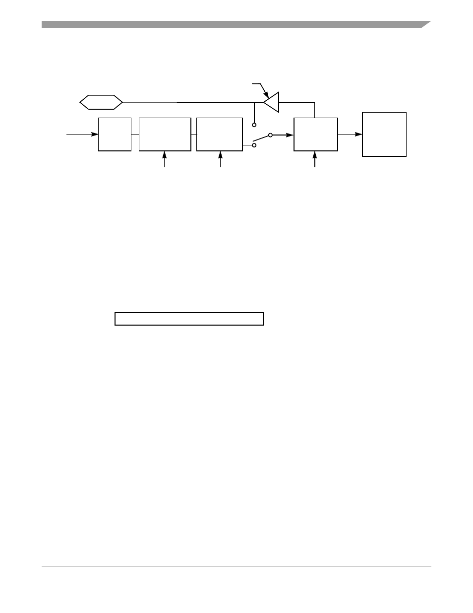
user’s responsibility to select the proper clock rate within the range as defined in the I
2
C and SPI bus
specifications.
Figure 7-2 SHI Clock Generator
7.4
Serial Host Interface Programming Model
The Serial Host Interface programming model has two parts:
•
Host side
—see
Section 7.4.1, "SHI Input/Output Shift Register
•
DSP side
—see
Section 7.4.2, "SHI Host Transmit Data Register (HTX)—DSP
through
Section 7.4.6, "SHI Control/Status Register (HCSR)—DSP Side"
information.
Figure 7-3 SHI Programming Model—Host Side
SHI
HMST
HMST = 0
HMST = 1
SCK/SCL
Divide By
1 or 8
Divide By 1
To
Divide By 256
HRS
HDM0–HDM7
SHI Clock
F
OSC
Divide
By 2
Controller
Clock
Logic
CPHA, CPOL, HI
2
C
AA0417
0
I/O Shift Register (IOSR)
IOSR
23
AA0418