1 esai_1 multiplex control register (emuxr), Esai_1 multiplex control register (emuxr) -5, Figure 9-2 – Freescale Semiconductor DSP56366 User Manual
Page 205: Emuxr register -5, Table 9-1, Emuxr esa/esai_1 pin selection -5
ESAI_1 Programming Model
DSP56366 24-Bit Digital Signal Processor User Manual, Rev. 4
Freescale Semiconductor
9-5
The ESAI_1 also contains the GPIO Port E functionality, described in
. The following paragraphs give detailed descriptions of bits in the ESAI_1 registers that differ
in functionality from their descriptions in the ESAI Programming Model.
9.3.1
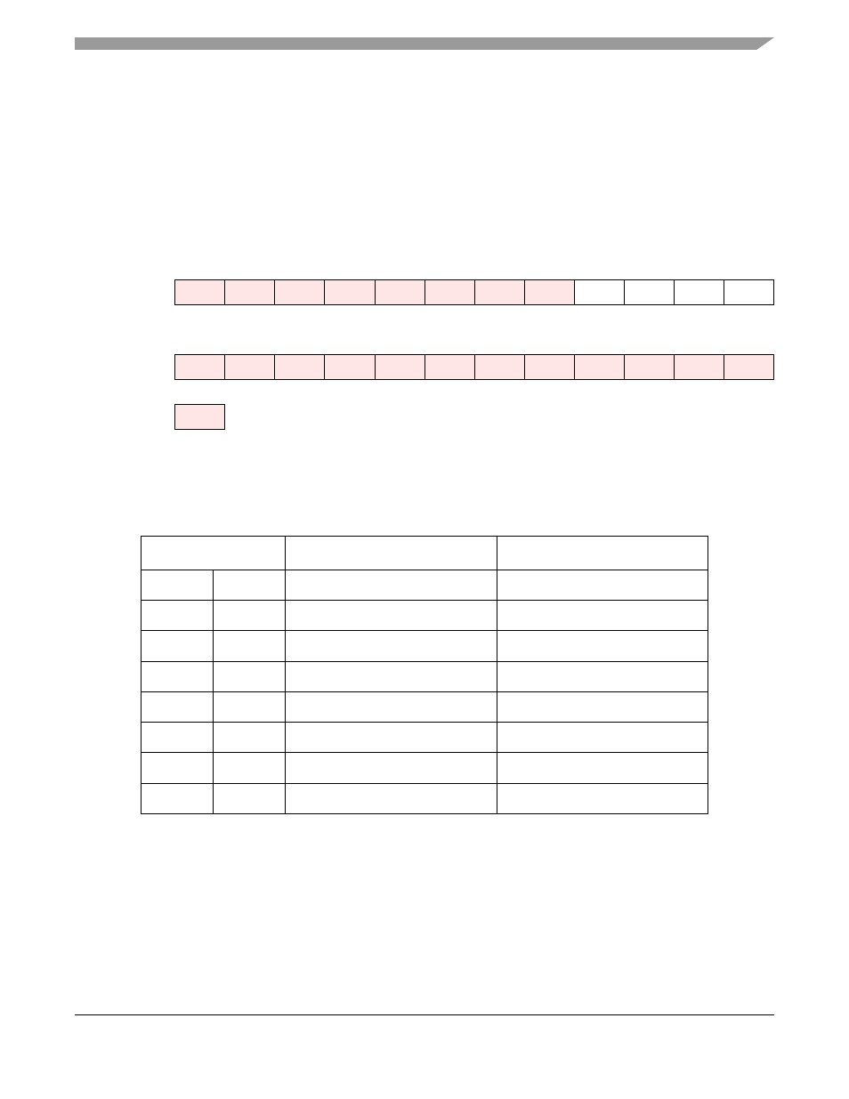
ESAI_1 Multiplex Control Register (EMUXR)
The read/write ESAI_1 Multiplex Control Register (EMUXR) controls which peripheral (ESAI or
ESAI_1) is using the shared pins.
Hardware and software reset clear all the bits of the EMUXR register. The selection of ESAI/ESAI_1 pins
is shown in
9.3.2
ESAI_1 Transmitter Clock Control Register (TCCR_1)
The read/write Transmitter Clock Control Register (TCCR_1) controls the ESAI_1 transmitter clock
generator bit and frame sync rates, the bit rate and high frequency clock sources and the directions of the
FST_1 and SCKT_1 signals. In synchronous mode, the bit clock defined for the transmitter determines the
receiver bit clock as well. TCCR_1 also controls the number of words per frame for the serial data.
Hardware and software reset clear all the bits of the TCCR_1 register.
11
10
9
8
7
6
5
4
3
2
1
0
Y:$FFFFAF
EMUX3 EMUX2 EMUX1 EMUX0
23
22
21
20
19
18
17
16
15
14
13
12
Reserved bit - read as zero; should be written with zero for future compatibility.
Figure 9-2 EMUXR Register
Table 9-1 EMUXR ESA/ESAI_1 Pin Selection
EMUXR bit
ESAI pin
ESAI_1 pin
EMUX0
0
SDO0 [PC11]
disconnected
EMUX0
1
disconnected
SDO0_1 [PE11]
EMUX1
0
SDO1[PC10]
disconnected
EMUX1
1
disconnected
SDO1_1 [PE10]
EMUX2
0
SDO2/SDI3 [PC9]
disconnected
EMUX2
1
disconnected
SDO2_1/SDI3_1 [PE9]
EMUX3
0
SDO3/SDI2 [PC8]
disconnected
EMUX3
1
disconnected
SDO3_1/SDI2_1 [PE8]