12 esai_1 time slot register (tsr_1), 13 transmit slot mask registers (tsma_1, tsmb_1), 14 receive slot mask registers (rsma_1, rsmb_1) – Freescale Semiconductor DSP56366 User Manual
Page 212: Esai_1 time slot register (tsr_1) -12, Transmit slot mask registers (tsma_1, tsmb_1) -12, Receive slot mask registers (rsma_1, rsmb_1) -12, Figure 9-11, Tsma_1 register -12, Figure 9-12, Tsmb_1 register -12
ESAI_1 Programming Model
DSP56366 24-Bit Digital Signal Processor User Manual, Rev. 4
9-12
Freescale Semiconductor
9.3.12
ESAI_1 Time Slot Register (TSR_1)
The write-only Time Slot Register (TSR_1) is effectively a null data register that is used when the data is
not to be transmitted in the available transmit time slot. The transmit data pins of all the enabled
transmitters are in the high-impedance state for the respective time slot where TSR_1 has been written.
The Transmitter External Buffer Enable pin (FSR_1 pin when SYN=1, TEBE=1, RFSD=1) disables the
external buffers during the slot when the TSR_1 register has been written.
9.3.13
Transmit Slot Mask Registers (TSMA_1, TSMB_1)
The Transmit Slot Mask Registers (TSMA_1 and TSMB_1) are two read/write registers used by the
transmitters in network mode to determine for each slot whether to transmit a data word and generate a
transmitter empty condition (TDE=1), or to tri-state the transmitter data pins. TSMA_1 and TSMB_1
should each be considered as containing half a 32-bit register TSM_1. See
and
Bit number N in TSM_1 (TS**) is the enable/disable control bit for transmission in slot number N.
9.3.14
Receive Slot Mask Registers (RSMA_1, RSMB_1)
The Receive Slot Mask Registers (RSMA_1 and RSMB_1) are two read/write registers used by the
receiver in network mode to determine for each slot whether to receive a data word and generate a receiver
full condition (RDF=1), or to ignore the received data. RSMA_1 and RSMB_1 should be considered as
each containing half of a 32-bit register RSM_1. See
RSM_1 (RS**) is an enable/disable control bit for receiving data in slot number N.
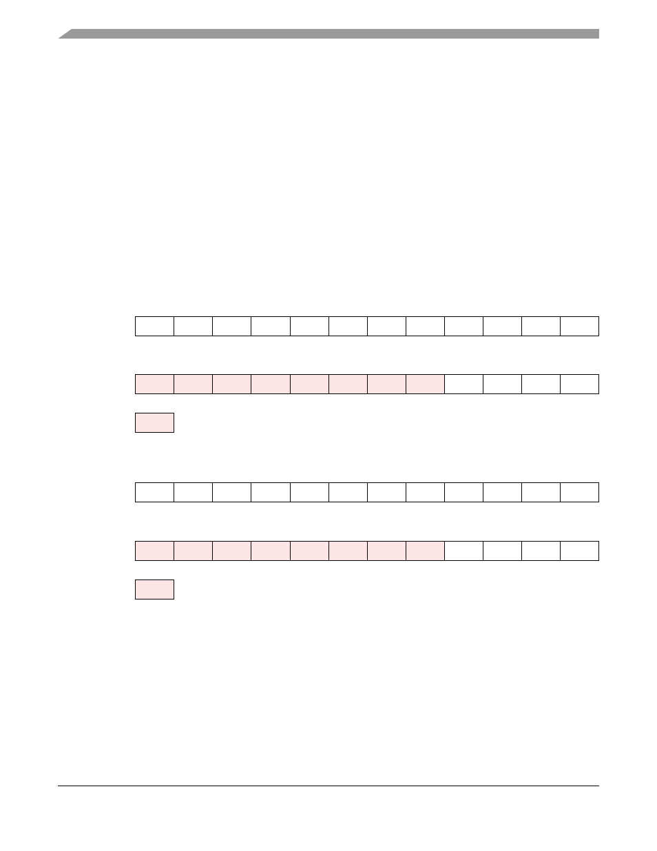
11
10
9
8
7
6
5
4
3
2
1
0
Y:$FFFF99
TS11
TS10
TS9
TS8
TS7
TS6
TS5
TS4
TS3
TS2
TS1
TS0
23
22
21
20
19
18
17
16
15
14
13
12
TS15
TS14
TS13
TS12
Reserved bit - read as zero; should be written with zero for future compatibility.
Figure 9-11 TSMA_1 Register
11
10
9
8
7
6
5
4
3
2
1
0
Y:$FFFF9A
TS27
TS26
TS25
TS24
TS23
TS22
TS21
TS20
TS19
TS18
TS17
TS16
23
22
21
20
19
18
17
16
15
14
13
12
TS31
TS30
TS29
TS28
Reserved bit - read as zero; should be written with zero for future compatibility.
Figure 9-12 TSMB_1 Register