Figure 8-15, Tsma register -41, Figure 8-16 – Freescale Semiconductor DSP56366 User Manual
Page 191: Tsmb register -41
ESAI Programming Model
DSP56366 24-Bit Digital Signal Processor User Manual, Rev. 4
Freescale Semiconductor
8-41
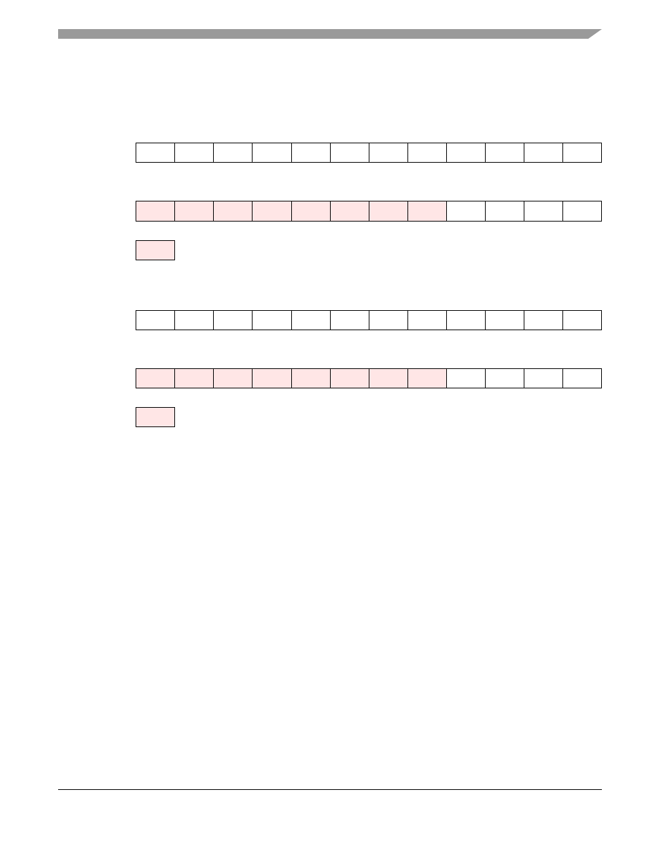
transmitter empty condition (TDE=1), or to tri-state the transmitter data pins. TSMA and TSMB should
each be considered as containing half a 32-bit register TSM. See
. Bit number
N in TSM (TS**) is the enable/disable control bit for transmission in slot number N.
When bit number N in TSM is cleared, all the transmit data pins of the enabled transmitters are tri-stated
during transmit time slot number N. The data is still transferred from the transmit data registers to the
transmit shift registers but neither the TDE nor the TUE flags are set. This means that during a disabled
slot, no transmitter empty interrupt is generated. The DSP is interrupted only for enabled slots. Data that
is written to the transmit data registers when servicing this request is transmitted in the next enabled
transmit time slot.
When bit number N in TSM register is set, the transmit sequence is as usual: data is transferred from the
TX registers to the shift registers, transmitted during slot number N, and the TDE flag is set.
Using the slot mask in TSM does not conflict with using TSR. Even if a slot is enabled in TSM, the user
may chose to write to TSR instead of writing to the transmit data registers TXx. This causes all the transmit
data pins of the enabled transmitters to be tri-stated during the next slot.
Data written to the TSM affects the next frame transmission. The frame being transmitted is not affected
by this data and would comply to the last TSM setting. Data read from TSM returns the last written data.
After hardware or software reset, the TSM register is preset to $FFFFFFFF, which means that all 32
possible slots are enabled for data transmission.
11
10
9
8
7
6
5
4
3
2
1
0
X:$FFFFB9
TS11
TS10
TS9
TS8
TS7
TS6
TS5
TS4
TS3
TS2
TS1
TS0
23
22
21
20
19
18
17
16
15
14
13
12
TS15
TS14
TS13
TS12
Reserved bit - read as zero; should be written with zero for future compatibility.
Figure 8-15 TSMA Register
11
10
9
8
7
6
5
4
3
2
1
0
X:$FFFFBA
TS27
TS26
TS25
TS24
TS23
TS22
TS21
TS20
TS19
TS18
TS17
TS16
23
22
21
20
19
18
17
16
15
14
13
12
TS31
TS30
TS29
TS28
Reserved bit - read as zero; should be written with zero for future compatibility.
Figure 8-16 TSMB Register