Esai – Freescale Semiconductor DSP56366 User Manual
Page 340
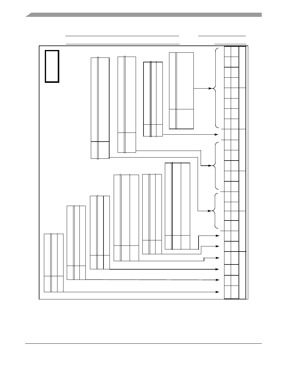
Programming Sheets
DSP56366 24-Bit Digital Signal Processor User Manual, Rev. 4
D-32
Freescale Semiconductor
Figure D-17. ESAI Receive Clock Control Register
15
6
5
4
19
18
17
16
10
9
8
7
14
13
12
11
RPM0
32
10
RPM2
23
22
21
20
RPM1
RPM
3
RPM4
RPM5
RPM6
RPM7
RPSR
RDC0
RDC1
RDC2
RDC3
RDC
4
RFP0
RFP1
RFP2
RFP3
RCKP
RFSP
RHCKP
RCKD
RFSD
RHC
KD
R
CKP
De
scrip
tion
0
1
Clockout on r
isin
g
ed
ge of
r
eceive
clock,
la
tc
h i
n
on
falling edge of
rece
iv
e clock
Clockout on f
alling edg
e
of
r
ecei
ve
cl
oc
k,
la
tc
h
in
on
ri
sing
edge
of receive
clo
ck
RFS
P
De
scription
0
1
Fr
am
e sync p
olar
ity
posit
ive
Fr
am
e sync p
olar
ity
nega
tive
RFP [
3:0]
D
escri
pti
on
Se
ts div
ide r
ate for r
ecei
ver
high fr
equency
cl
ock
RCKD
Desc
rip
ti
o
n
0
1
Exter
nal clock source us
ed
In
te
rnal cloc
k
so
ur
ce
RFSD
De
sc
ri
ption
0
1
FSR
is in
put
FSR is ou
tpu
t
RH
CKD
D
escr
iption
0
1
HC
KR
is
input
HC
KR
is
o
utput
RH
CK
P
D
escription
0
1
Clockout on r
ising
ed
ge of
r
eceive
clock,
latch
in on f
all
in
g
edge of
r
eceive
clock
C
loc
kou
t on falling
ed
ge
of
rec
eiv
e
cl
ock
,
latch
in on r
ising edge of
receive clock
Range $0 -
$F (
1 -
16). Se
e 8.3.3.4
RD
C [4
:0
]
D
es
c
ri
p
ti
on
C
ontro
ls
fr
a
m
e
rate
dividers
R
P
M [7
:0]
D
escription
S
pecifies prescaler rat
io
for
th
e
RPSR
Desc
ript
ion
0
1
Div
ide by
8
pres
ca
le
r o
per
at
io
nal
Div
ide by
8
pres
ca
le
r b
yp
as
sed
Ra
nge
fr
om
$0
0 - $
FF (
1 - 25
6)
.
re
ceive clock
generat
or
S
ee 8.
3.3.1
ESAI
RCCR - ESAI Receive Cl
ock Control Register
X: $FFFFB8 Reset: $000000
Ran
ge
00000 -
1111
1
(1-
32)
See
8.3.3.2
Application:
Date:
Programmer: