13 receive slot mask registers (rsma, rsmb), Receive slot mask registers (rsma, rsmb) -42, Figure 8-17 – Freescale Semiconductor DSP56366 User Manual
Page 192: Rsma register -42, Figure 8-18, Rsmb register -42
ESAI Programming Model
DSP56366 24-Bit Digital Signal Processor User Manual, Rev. 4
8-42
Freescale Semiconductor
NOTE
When operating in normal mode, bit 0 of the mask register must be set,
otherwise no output is generated.
8.3.13
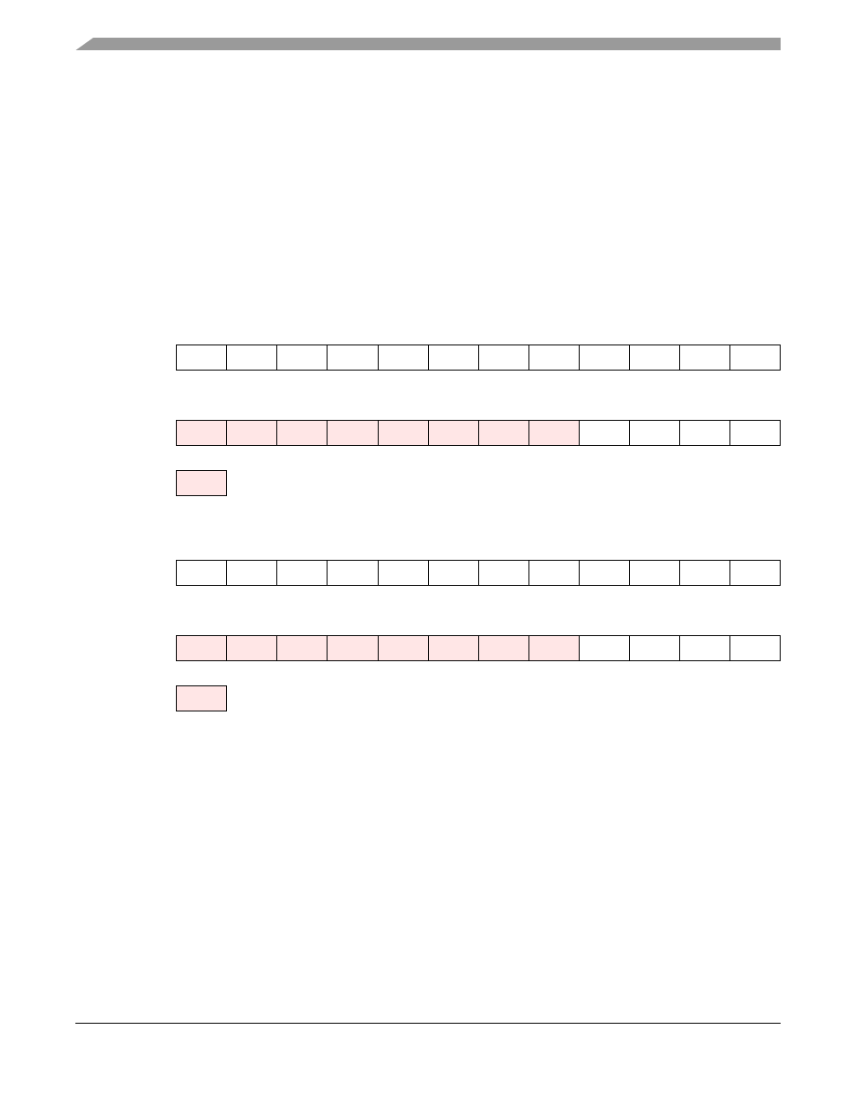
Receive Slot Mask Registers (RSMA, RSMB)
The Receive Slot Mask Registers (RSMA and RSMB) are two read/write registers used by the receiver in
network mode to determine for each slot whether to receive a data word and generate a receiver full
condition (RDF=1), or to ignore the received data. RSMA and RSMB should be considered as each
containing half of a 32-bit register RSM. See
and
. Bit number N in RSM (RS**)
is an enable/disable control bit for receiving data in slot number N.
When bit number N in the RSM register is cleared, the data from the enabled receivers input pins are
shifted into their receive shift registers during slot number N. The data is not transferred from the receive
shift registers to the receive data registers, and neither the RDF nor the ROE flags are set. This means that
during a disabled slot, no receiver full interrupt is generated. The DSP is interrupted only for enabled slots.
When bit number N in the RSM is set, the receive sequence is as usual: data which is shifted into the
enabled receivers shift registers is transferred to the receive data registers and the RDF flag is set.
Data written to the RSM affects the next received frame. The frame being received is not affected by this
data and would comply to the last RSM setting. Data read from RSM returns the last written data.
After hardware or software reset, the RSM register is preset to $FFFFFFFF, which means that all 32
possible slots are enabled for data reception.
11
10
9
8
7
6
5
4
3
2
1
0
X:$FFFFBB
RS11
RS10
RS9
RS8
RS7
RS6
RS5
RS4
RS3
RS2
RS1
RS0
23
22
21
20
19
18
17
16
15
14
13
12
RS15
RS14
RS13
RS12
Reserved bit - read as zero; should be written with zero for future compatibility.
Figure 8-17 RSMA Register
11
10
9
8
7
6
5
4
3
2
1
0
X:$FFFFBC
RS27
RS26
RS25
RS24
RS23
RS22
RS21
RS20
RS19
RS18
RS17
RS16
23
22
21
20
19
18
17
16
15
14
13
12
RS31
RS30
RS29
RS28
Reserved bit - read as zero; should be written with zero for future compatibility.
Figure 8-18 RSMB Register