2 individual timer block diagram, Individual timer block diagram -2, Figure 11-1 – Freescale Semiconductor DSP56366 User Manual
Page 232: Timer/event counter block diagram -2
Timer/Event Counter Architecture
DSP56366 24-Bit Digital Signal Processor User Manual, Rev. 4
11-2
Freescale Semiconductor
11.2.2
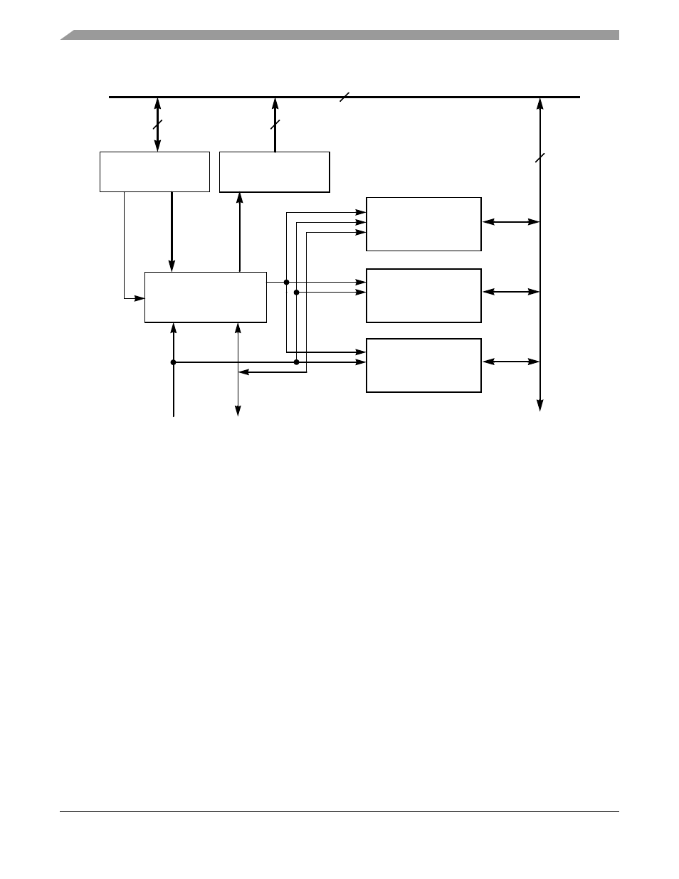
Individual Timer Block Diagram
shows the structure of an individual timer module. The three timers are identical in structure,
but only timer 0 is externally accessible.
Each timer includes a 24-bit counter, a 24-bit read/write timer control and status register (TCSR), a 24-bit
read-only timer count register (TCR), a 24-bit write-only timer load register (TLR), a 24-bit read/write
timer compare register (TCPR), and logic for clock selection and interrupt/DMA trigger generation.
The timer mode is controlled by the TC[3:0] bits of the timer control/status register (TCSR). Timer modes
are described in
Section 11.4, "Timer Modes of Operation"
Figure 11-1 Timer/Event Counter Block Diagram
Timer Prescaler
Count Register
GDB
24
24
TPLR
24
Timer 0
Timer 2
Timer 1
21-bit Prescaler
CLK/2
TPCR
Timer Prescaler
Load Register
24
Counter
AA0673
TIO0