2 port e direction register (prre), 3 port e data register (pdre), Port e direction register (prre) -14 – Freescale Semiconductor DSP56366 User Manual
Page 214: Port e data register (pdre) -14, Figure 9-15, Pcre register -14, Figure 9-16, Prre register -14, Table 9-4, Pcre and prre bits functionality -14
GPIO - Pins and Registers
DSP56366 24-Bit Digital Signal Processor User Manual, Rev. 4
9-14
Freescale Semiconductor
9.5.2
Port E Direction Register (PRRE)
The read/write 24-bit Port E Direction Register (PRRE) in conjunction with the Port E Control Register
(PCRE) controls the functionality of the ESAI_1 GPIO pins.
describes the port pin
configurations. Hardware and software reset clear all PRRE bits.
9.5.3
Port E Data register (PDRE)
The read/write 24-bit Port E Data Register (see
) is used to read or write data to/from ESAI_1
GPIO pins. Bits PD(11:0) are used to read or write data from/to the corresponding port pins if they are
configured as GPIO. If a port pin [i] is configured as a GPIO input, then the corresponding PD[i] bit will
reflect the value present on this pin. If a port pin [i] is configured as a GPIO output, then the value written
into the corresponding PD[i] bit will be reflected on this pin. If a port pin [i] is configured as disconnected,
the corresponding PD[i] bit is not reset and contains undefined data.
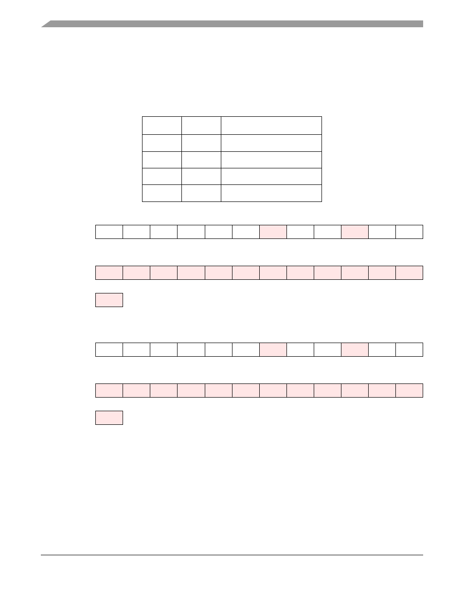
Table 9-4 PCRE and PRRE Bits Functionality
PDE[i]
PE[i]
Port Pin[i] Function
0
0
disconnected
0
1
GPIO input
1
0
GPIO output
1
1
ESAI_1
11
10
9
8
7
6
5
4
3
2
1
0
Y:$FFFF9F
PE11
PE10
PE9
PE8
PE7
PE6
PE4
PE3
PE1
PE0
23
22
21
20
19
18
17
16
15
14
13
12
Reserved bit - read as zero; should be written with zero for future compatibility.
Figure 9-15 PCRE Register
11
10
9
8
7
6
5
4
3
2
1
0
Y:$FFFF9E
PDE11 PDE10
PDE9
PDE8
PDE7
PDE6
PDE4
PDE3
PDE1
PDE0
23
22
21
20
19
18
17
16
15
14
13
12
Reserved bit - read as zero; should be written with zero for future compatibility.
Figure 9-16 PRRE Register