Figure d-2, Central processor – Freescale Semiconductor DSP56366 User Manual
Page 325
Programming Sheets
DSP56366 24-Bit Digital Signal Processor User Manual, Rev. 4
Freescale Semiconductor
D-17
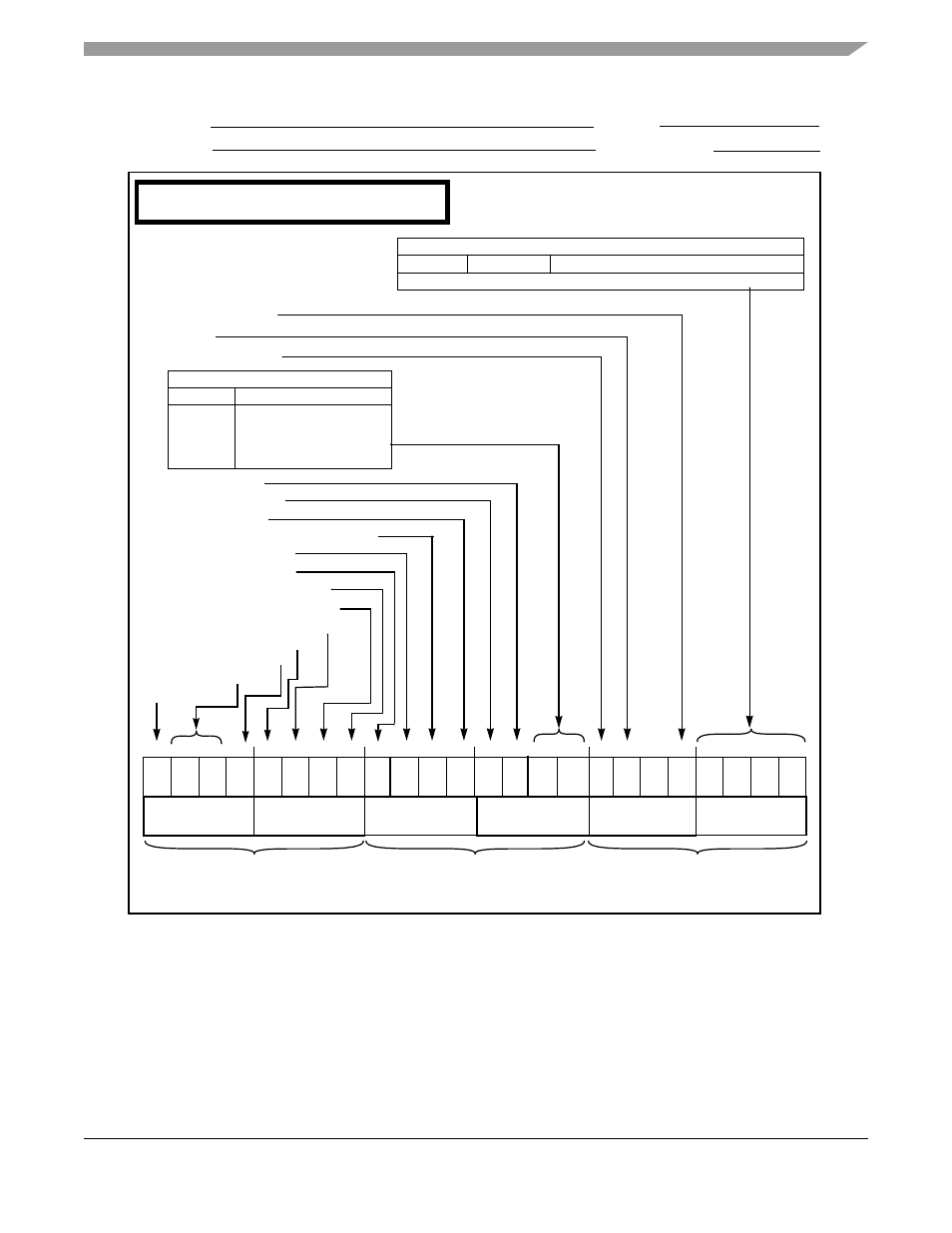
Figure D-2. Operating Mode Register (OMR)
Chip Operating Modes
MOD(D:A) Reset Vector
Description
See Core Configuration Section.
Application
:
Date:
Programmer:
Sheet 2 of 5
15 14 13 12
11 10
9
8
7
6
5
4
3
2
1
0
EBD
MC
MB
MA
19 18 17 16
23 22
21 20
SD
BRT TAS
SEN
CDP1CDP0
WRP EOV EUN XYS
BE
MD
Core-DMA Priority
CDP(1:0)
Core-DMA Priority
00
01
10
11
Core vs DMA Priority
DMA accesses > Core
DMA accesses = Core
DMA accesses < Core
MSW1
MSW0
*
0
Chip Operating Mode
Register (COM)
System Stack Control
Status Register (SCS)
Extended Chip Operating
Mode Register (COM)
Operating Mode Register (OMR)
Read/Write Reset = $00030X
Central Processor
*
= Reserved, Program as 0
Burst Mode Enable
TA Synchronize Select
Bus Release Timing
Stack Extension Space Select
Extended Stack Underflow Flag
Extended Stack Overflow Flag
Extended Stack Wrap Flag
Stack Extension Enable
Memory Switch Mode
MS
External Bus Disable
Stop Delay
Memory Switch Mode
PEN
ATE APD
Address Priority Disable
Address Tracing Enable
ABE
Asynchronous Bus Arbitration Enable
Patch Enable