8 host data register (hdr), 9 dsp-side registers after reset, Host data register (hdr) -16 – Freescale Semiconductor DSP56366 User Manual
Page 110: Dsp-side registers after reset -16, Figure 6-9, Figure 6-10, Host data register (hdr) (x:$ffffc9) -16, Table 6-6, Hdr and hddr functionality -16
HDI08 – DSP-Side Programmer’s Model
DSP56366 24-Bit Digital Signal Processor User Manual, Rev. 4
6-16
Freescale Semiconductor
6.5.8
Host Data Register (HDR)
The HDR register holds the data value of the corresponding bits of the HDI08 pins which are configured
as GPIO pins. The functionality of the Dxx bit depends on the corresponding HDDR bit (DRxx). See
6.5.9
DSP-Side Registers After Reset
shows the results of the four reset types on the bits in each of the HDI08 registers accessible by
the DSP core. The hardware reset (HW) is caused by the RESET signal. The software reset (SW) is caused
by executing the RESET instruction. The individual reset (IR) is caused by clearing the HEN bit (HPCR
bit 6). The stop reset (ST) is caused by executing the STOP instruction.
15
14
13
12
11
10
9
8
7
6
5
4
3
2
1
0
DR15
DR14
DR13
DR12
DR11
DR10
DR9
DR8
DR7
DR6
DR5
DR4
DR3
DR2
DR1
DR0
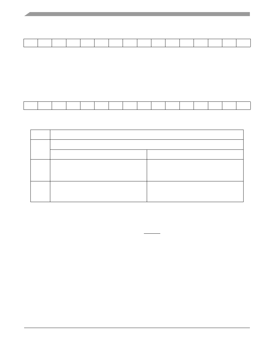
Figure 6-9 Host Data Direction Register (HDDR) (X:$FFFFC8)
15
14
13
12
11
10
9
8
7
6
5
4
3
2
1
0
D15
D14
D13
D12
D11
D10
D9
D8
D7
D6
D5
D4
D3
D2
D1
D0
Figure 6-10 Host Data Register (HDR) (X:$FFFFC9)
Table 6-6 HDR and HDDR Functionality
HDDR
HDR
DRxx
Dxx
GPIO pin
1
1
Defined by the selected configuration
non-GPIO pin
0
Read only bit. The value read is the binary value of
the pin.
The corresponding pin is configured as an input.
Read only bit. Does not contain significant data.
1
Read/write bit. The value written is the value read.
The corresponding pin is configured as an output, and
is driven with the data written to Dxx.
Read/write bit. The value written is the value read.