Comtech EF Data SDM-650B User Manual
Page 67
SDM-650B Satellite Modem
Configuration
Rev. 5
3–25
DS-1 LINE
TO BUFFER
OPTIONS
TX CLOCK
DS-1
DEJITTER
RECEIVER/
DRIVER
T
E
R
R
E
S
T
R
I
A
L
SD
RD
LOOPBACK CONTROL
M
O
D
E
M
TX DATA
RX CLOCK
RX DATA
MC
EXTERNAL BUFFER CLOCK
TO BUFFER
COMMON EQUIPMENT
OPTIONS
LOGIC
CONTROL
FAULT
RELAYS
MODULATOR
DEMODULATOR
DATA BUS TO M & C
TTL MODULATOR FAULT
TTL DEMODULATOR FAULT
N X 64 KB
CLOCK
SYNTHESIZER
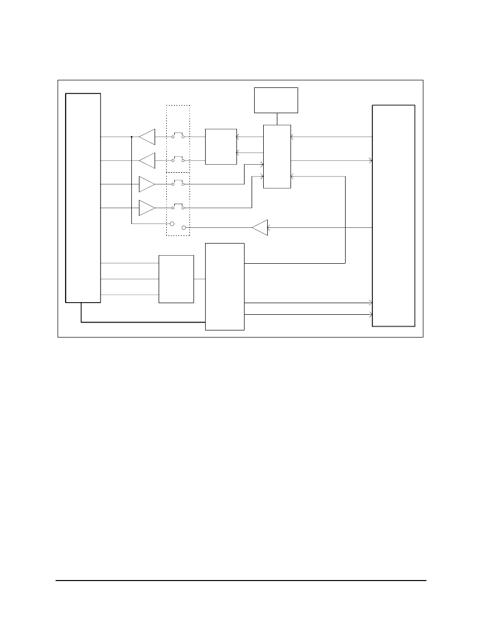
Figure 3-9. G.703 2048 Interface Block Diagram
The G.703 2048 kbit/s interface will operate in AMI, enabled by SW1-8.
The data to be transmitted by the modem is input on the SD lines. Jitter on the SD is
removed by a FIFO and clock recovery phase-locked loop. Data received and
demodulated by the modem is output on the RD lines.
The G.703 2048 kbit/s interface provides bi-directional loopback of the data at the DCE
interface. In loopback from the DTE side, SD is connected to RD. From the modem side,
the received demodulated data is routed back to the modulator input for re-transmission.
Three fault outputs are provided on dry contact FORM C relays:
• Common
Equipment
• Modulator
• Demodulator