Comtech EF Data SDM-650B User Manual
Page 299
SDM-650B Satellite Modem
Trojan Interface
Rev. 5
G–3
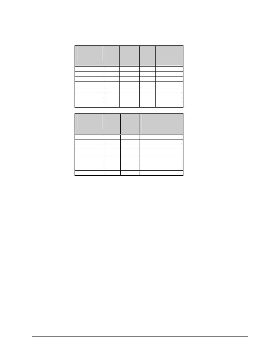
Receive
Data Rate
(kbit/s)
N
K
L
Receive
VCO
Frequency
(kHz)
56 7
64
7
3584
64 8
64
8
4096
128 16
32
16 4096
256 32
16
32 4096
512 64
8
64 4096
1024 128 4 128 4096
1544 193 2 193 3088
2048 256 2 256 4096
Receive
Data Rate
(kbit/s)
K
L
Receive
VCO
Frequency
(kHz)
56 64
7
3584
64 64
8
4096
128 32
16
4096
256 16
32
4096
512 8
64
4096
1024 4
128
4096
1544 2
193
3088
2048 2
256
4096
The MIL-STD-188-114 interface provides a Send Timing (ST) clock signal at the modem
transmit data rate. In the INTERNAL clock mode, the data to be transmitted, Send Data
(SD), must be synchronized to ST. In the EXTERNAL clock mode, clock is accepted on
the Terminal Timing input (TT) to clock in the data to be transmitted. In either case, the
phase relationship between the clock and data is not important, so long as it meets the
jitter specifications of MIL-STD-188-100, because a clock phase correction circuit is
provided, which shifts the clock away from the data transition times. If EXTERNAL
clock mode is used, the clock must be long-term synchronous with the synthesizer
reference, unless it is selected to “Transmit” clock.
Data received by the modem is output on the Receive Data (RD) lines, while the
recovered clock is output on the Receive Timing (RT) lines. For applications that require
the rising edge of the clock to occur in the middle of the data bit time, Receive Clock
NORMAL mode should be selected. INVERT mode puts the falling edge of RT in the
middle of the data bit.
The Request to Send (RS) lines are hard-wired to the Clear to Send (CS) lines, since the
modem does not support polled operation.
Data Mode (DM) indicates that the modem is powered up.