Figure g-1. trojan interface block diagram – Comtech EF Data SDM-650B User Manual
Page 298
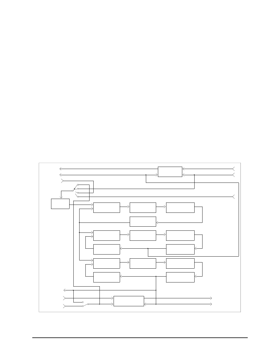
Trojan Interface
SDM-650B Satellite Modem
G–2
Rev. 5
The data rate synthesizer may take its input reference clock (REF_CLK) from one of four
different sources:
• Transmit
clock
• Receive
clock
• External Station Clock (MC)
• Internal clock (SCT)
The phase-lock loop which locks to the reference has a very narrow bandwidth,
effectively dejittering the reference. The phase-lock loop can handle data rates from
32 kbit/s to 2.048 Mbit/s, in steps of 8 kHz. Transmit and receive data rates do not need
to be the same. If used, External Station Clock may range from 32 kHz to 10 MHz, in
steps of 8 kHz.
The Doppler buffer depth ranges from 512 to 32768 bits, in powers of 2. The buffer is
centered on power-up, start of service (when the modem receive section locks), or in case
of underflow or overflow. The buffer may also be centered manually. Buffer overflow
and underflow are logged as stored faults so that clock offset information may be
obtained.
MODEM RX CLOCK
MODEM RX DATA
DOPPLER
BUFFER
RX DATA
TO CUSTOMER
RX CLOCK
TO CUSTOMER
STATION
REFERENCE
MODEM SCT CLOCK
4.096 MHZ
DEJITTERED
VOLTAGE
CONTROLLED XTAL
OSCILLATOR
RECEIVE
CLOCK LOOP
FILTER
RECEIVE
CLOCK LOOP
PHASE DETECTOR
8 KHZ
8 KHZ
DIVIDE
BY
N
8 KHZ
8 KHZ
DIVIDE
BY
512
VCO FREQUENCY
(SEE TABLE)
DEJITTERED
RECEIVE
VOLTAGE
CONTROLLED
OSCILLATOR
DIVIDE
BY
K
RECEIVE
CLOCK LOOP
FILTER
RECEIVE
CLOCK LOOP
PHASE DETECTOR
DIVIDE
BY
L
8 KHZ
8 KHZ
RECEIVE
CLOCK LOOP
PHASE DETECTOR
RECEIVE
CLOCK LOOP
FILTER
VOLTAGE
CONTROLLED
OSCILLATOR
VCO FREQUENCY
(SEE TABLE)
DEJITTERED
TRANSMIT
DIVIDE
BY
M
DIVIDE
BY
P
TX DATA RATE
CLOCK
TO CUSTOMER
TX DATA
FROM CUSTOMER
TX CLOCK
FROM CUSTOMER
INT/EXT
TX CLOCK
FIFO
BUFFER
MODEM TX DATA
MODEM TX CLOCK
Figure G-1. Trojan Interface Block Diagram