Mo d e m – Comtech EF Data SDM-650B User Manual
Page 63
SDM-650B Satellite Modem
Configuration
Rev. 5
3–21
DS-1 LINE
TO BUFFER
OPTIONS
TX CLOCK
DS-1
DEJITTER
RECEIVER/DRIVER
T
E
R
R
E
S
T
R
I
A
L
SD
RD
LOOPBACK CONTROL
M
O
D
E
M
TX DATA
RX CLOCK
RX DATA
MC
EXTERNAL BUFFER CLOCK
TO BUFFER
COMMON EQUIPMENT
OPTIONS
LOGIC
CONTROL
FAULT
RELAYS
MODULATOR
DEMODULATOR
DATA BUS TO M & C
TTL MODULATOR FAULT
TTL DEMODULATOR FAULT
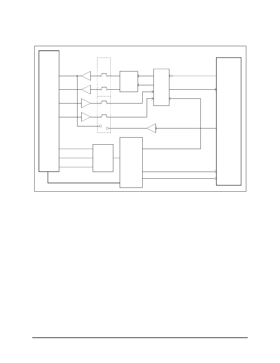
Figure 3-7. DS-1 Interface Block Diagram
The data to be transmitted by the modem is input on the SD lines. Jitter on the SD is
removed by a FIFO and clock recovery phase-locked loop. Data received and
demodulated by the modem is output on the RD lines.
The RD is driven from a pulse-shaper circuit which pre-equalizes the RD output to drive
up to 655 feet of ABAM cable. Refer to Table 3-3.
The DS-1 interface provides bi-directional loopback of the data at the DCE interface.
In loopback from the DTE side, SD is connected to RD.
In loopback from the modem side, the received demodulated data is routed back to the
modulator input for re-transmission.
- CDD-880 (124 pages)
- CDM-800 (130 pages)
- ODMR-840 (184 pages)
- CDM-750 (302 pages)
- CDM-840 (244 pages)
- SLM-5650A (420 pages)
- CTOG-250 (236 pages)
- CDM-700 (256 pages)
- CDM-760 (416 pages)
- CDM-710G (246 pages)
- CDM-600/600L (278 pages)
- CDMR-570L (512 pages)
- CDM-625 (684 pages)
- CDM-625A (756 pages)
- CDD-564A (240 pages)
- CDD-564L (254 pages)
- CLO-10 (134 pages)
- MCED-100 (96 pages)
- CDMR-570AL (618 pages)
- CDM-600 LDPC (2 pages)
- BUC Power Supply Ground Cable (2 pages)
- MPP70 Hardware Kit for CDM-570L (4 pages)
- MPP50 Hardware Kit for CDM-570L (4 pages)
- CDM-625 DC-AC Conversion (4 pages)
- CDM-625 DC-AC Conversion with IP Packet Processor (4 pages)
- DMDVR20 LBST Rev 1.1 (117 pages)
- DMD2050E (212 pages)
- DMD-2050 (342 pages)
- DMD1050 (188 pages)
- OM20 (220 pages)
- QAM256 (87 pages)
- DD240XR Rev Е (121 pages)
- MM200 ASI Field (5 pages)
- DM240-DVB (196 pages)
- MM200 (192 pages)
- CRS-150 (78 pages)
- CRS-280L (64 pages)
- CRS-170A (172 pages)
- CRS-180 (136 pages)
- SMS-301 (124 pages)
- CiM-25/8000 (186 pages)
- CiM-25 (26 pages)
- CRS-500 (218 pages)
- CRS-311 (196 pages)
- CIC-20 LVDS to HSSI (26 pages)