G.3 specification, G.3.1 mil-std-188-114 parameters, G.3.2 clock synthesizer/dejitter circuit – Comtech EF Data SDM-650B User Manual
Page 302: G.3.3 doppler buffer parameters
Trojan Interface
SDM-650B Satellite Modem
G–6
Rev. 5
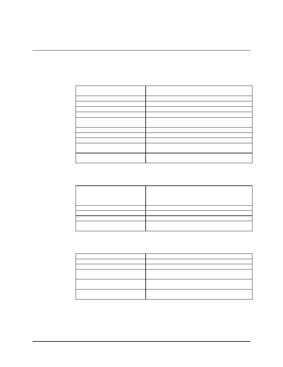
G.3 Specification
G.3.1 MIL-STD-188-114 Parameters
Circuit Supported
SD, ST, TT, RD, RT, DM, RR, MC, MOD FAULT,
DEMOD FAULT.
Amplitude (RD, RT, ST, DM, RR)
4, ± 2V differential into 100
Ω.
DC Offset (RD, RT, ST, DM, RR)
± 0.4V.
Impedance (RD, RT, ST, DM, RR)
Less than 100
Ω, differential.
Impedance (SD, TT, MC)
100, ± 20
Ω, differential.
Polarity
True when B positive with respect to A.
False when A positive with respect to B.
Phasing (TT, RT)
False-to-true transition nominally in center of data bit.
Symmetry (ST, TT, RT)
50%, ± 5%.
Frequency Stability (ST)
± 100 ppm.
Modulator Fault
Open collector output, 15V max, 20 mA max current
sink. Fault is open circuit.
Demodulator Fault
Open collector output, 15V max, 20 mA max current
sink. Fault is open circuit.
G.3.2 Clock Synthesizer/Dejitter Circuit
Reference Clk Sources
Transmit Clk
Receive Data Clk
External Reference Clk (MC)
Modem Internal Clk (SCT)
Reference Clk Input
32 kHz to 10 MHz, in 8 kHz steps
Synthesized TX Clock
56 to 2048 kHz, in 8 kHz steps
Synthesized RX Clock
56 to 2048 kHz, in 8 kHz steps
Jitter Gain
Synth Clk Freq/Ref Clk Freq, modified by a 1-pole
(20 dB/decade) low-pass response corner at 0.4 Hz
G.3.3 Doppler Buffer Parameters
Buffer Size (bits)
512, 1024, 2048, 4096, 8192, 16384, 32768
Clock Source
Synthesized RX Clock
Data Rate
56 to 2048 kbit/s
Indicators
Buffer Overflow (stored fault)
Buffer Underflow (stored fault)
Controls
Reset Buffer to Center
Buffer Depth
Misc. Buffer
automatically
recenters on Over/Underflow,
power-on, or start of service