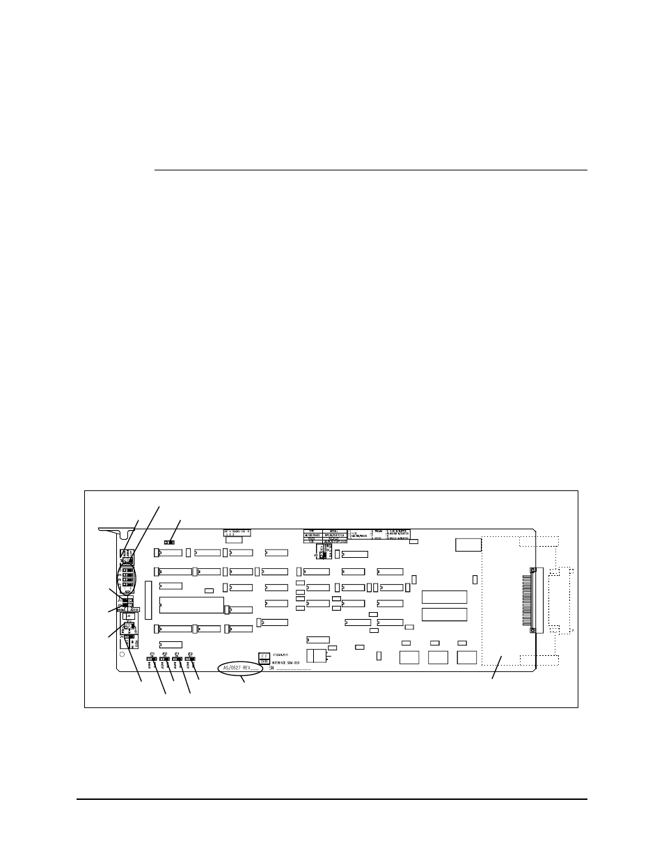
2 v.35 interface, Figure 3-4. v.35 interface card – Comtech EF Data SDM-650B User Manual
Page 56
Configuration
SDM-650B Satellite Modem
3–14
Rev.
5
3.2.2 V.35 Interface
3.2.2.1 Functional Description
The V.35 digital interface (Figure 3-4) provides level translation, buffering, and
termination between the internal modem signals and the V.35 DCE interface connector
on the rear panel.
Electrical characteristics of the interface signals are defined in CCITT Recommendation
V.35.
The electrical and mechanical specifications are summarized in Section 3.2.2.2 and
Section 3.2.2.3, respectively.
A functional block diagram of the V.35 interface is shown in Figure 3-5.
The V.35 interface provides a Serial Clock Transmit (SCT) clock signal at the modem
data rate.
In the Internal clock mode, the data to be transmitted, SD, must be synchronized to SCT.
In the External clock mode, the clock is accepted on the Serial Clock Transmit External
(SCTE) input to clock in the data to be transmitted.
JP2
JP12
JP13
JP14
JP15 ASSEMBLY NUMBER
AND REVISION
JP1
ADDRESS SELECT JUMPERS
JP16
V.35 ADAPTOR
CONNECTOR
JP3
JP8
JP10
Figure 3-4. V.35 Interface Card