2 sequential decoder/demodulator processor, Figure 5-3. decoder block diagram – Comtech EF Data SDM-650B User Manual
Page 131
SDM-650B Satellite Modem
Theory of Operation
Rev. 6
5–7
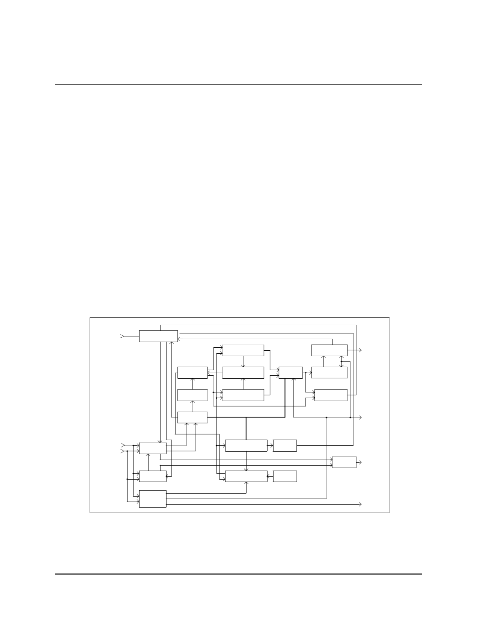
5.2 Sequential Decoder/Demodulator Processor
The modem sequential decoder/demodulator processor is a 10.25” x 14” card that fits in
the middle-left slot of the modem chassis.
The card performs five separate functions:
• Contains the digital Costas processor which provides signals to the demodulator
board for carrier recovery and Automatic Gain Control (AGC)
• Performs clock recovery of both the symbol clock and data clock
• Provides the FEC function utilizing a sequential decoder
• Provides differential decoding
• Provides V.35 descrambling
Refer to Figure 5-3 for a block diagram of the board. Refer to Section 5.2.2 for a detailed
description of the module.
MICRO-
COMPUTER
BUS
MICROCOMPUTER
INTERFACE
SYNDROME SHIFT
REGISTER A
V.35
DESCRAMBLER
RECEIVE
DATA
DIFFERENTIAL
DECODER
OUTPUT
BUFFER
PARITY
GENERATOR
SYNDROME
INPUT
GENERATOR
AMBIGUITY
RESOLVER
INPUT
BUFFER
SYNDROM SHIFT
REGISTER B
DETECTOR
RECEIVE
CHANNEL BER
CLOCK
LOCK
DETECT
ADDRESS
GENERATOR
COSTAS
PROCESSOR
I CHANNEL
Q CHANNEL
VCXO
SW EEP
TIMING AND
CONTROL
PROCESS
CLOCK
DDS
RCVR
IF
AGC
CONTROL
CLOCK
RECOVERY
Figure 5-3. Decoder Block Diagram