2 control register, Figure 3-4, Control register read format -4 – Epson ARM.POWERED ARM720T User Manual
Page 64: Figure 3-5, Control register write format -4, Control register, Control, Register
3: Configuration
3-4
EPSON
ARM720T CORE CPU MANUAL
3.3.2
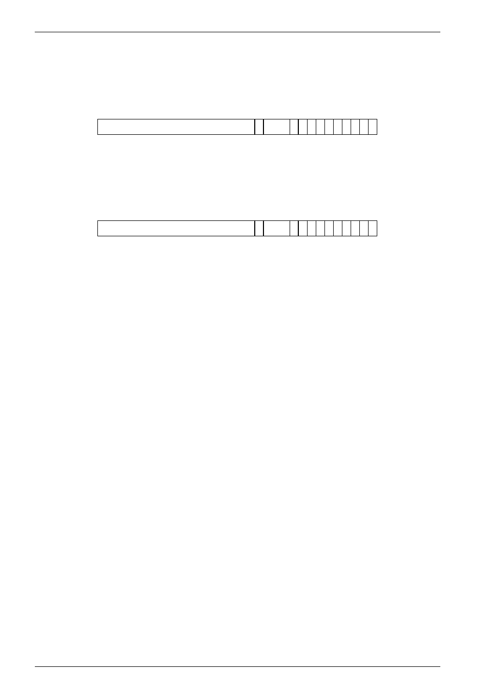
Control Register
Reading from CP15 Register 1 reads the control bits. The CRm and opcode_2 fields Should Be
Zero when reading CP15 Register 1. Control Register read format is shown in Figure 3-4.
Figure 3-4 Control Register read format
Writing to CP15 Register 1 sets the control bits. The CRm and opcode_2 fields Should Be Zero
when writing to CP15 Register 1. Control Register write format is shown in Figure 3-5.
Figure 3-5 Control Register write format
With the exception of the V bit, all defined control bits are set to zero on reset. The control bits
have the following functions:
M Bit 0
MMU enable/disable:
0 = MMU disabled
1 = MMU enabled.
A Bit 1
Alignment fault enable/disable:
0 = Address Alignment Fault Checking disabled
1 = Address Alignment Fault Checking enabled.
C Bit 2
Cache enable/disable:
0 = Instruction and/or Data Cache (IDC) disabled
1 = Instruction and/or Data Cache (IDC) enabled.
W Bit 3
Write buffer enable/disable:
0 = Write Buffer disabled
1 = Write Buffer enabled.
P Bit 4
When read, returns 1. When written, is ignored.
D Bit 5
When read, returns 1. When written, is ignored.
L Bit 6
When read, returns 1. When written, is ignored.
B Bit 7
Big-endian/little-endian:
0 = Little-endian operation
1 = Big-endian operation.
S Bit 8
System protection: Modifies the MMU protection system.
R Bit 9
ROM protection: Modifies the MMU protection system.
31
14 13 12 11 10 09 08 07 06 05 04 03 02 01 00
UNP
V
UNP
R S B L D P W C A M
31
14 13 12 11 10 09 08 07 06 05 04 03 02 01 00
UNP/SBZ
V
UNP/
SBZ
R S B L D P W C A M